 fl@C@
fl@C@
I always think ahead a bit... Starting with a rough idea, and gradually refining that until reality starts dictating the direction.. It's a balance I think most hackers battle with.. So, I had some grand ideas at the beginning of this project, and some misunderstandings of certain things, and a whole lot of research and learning has brought me a little closer..but I think that's what this whole thing is about.. It's all about learning and trying to do better. This project has definitely been a learning experience.. in multiple ways...and I continue to learn more and more..
So, having said all of that.. I have been upgrading my research efforts on how exactly I am going to tackle the final design of the spectrometer portion of this system.. There's certainly lots and lots of options.. My goals are to make it cheap, configurable, easy to build, and upgradable..
So.. There's some factors to consider.... What type of imaging device do I use? What type of optics do I use? How do I fit this all in and still make it work?
Well, in respect to which imaging device do I use.... I started out with the notion that I was going to use the raspberryPi camera and take multiple exposures, do some image stacking and so on... The tradeoff would turn out to be more significant than I originally thought.. Turns out factors such as the Bayer filter and noise would be a major limitation. I then turned my eye toward Linear CCD Array Detectors (Linear CCD).. As it turns out there are a couple that are most popular in spectrometers.. The Sony ILX511 and the Toshiba TCD1304AP.. From what I can see, it is relatively simple to interface to these devices.. The Sony from what I can tell is no longer in production (from what I can tell).. The Toshiba seems to be still around.. Both are not terribly easy to source...unless it is through eBay and is accompanied by a few weeks of waiting... At my stage in this project, and with the hackaday prize deadlines... I can't wait until September..
So, in a mad search today.. I discovered the AMS (formerly TAOS) TSL1410R..
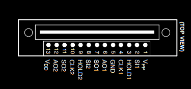
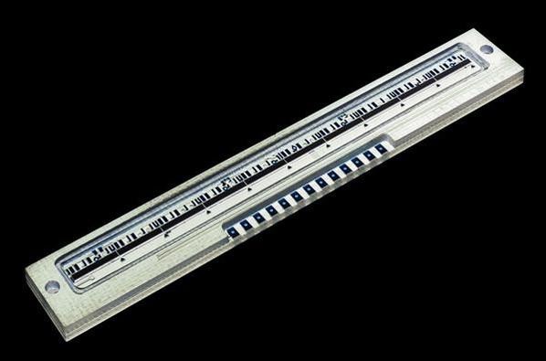
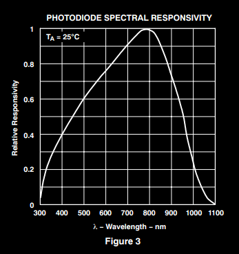
It isn't a CCD device.. Rather it is a diode sensor array.. It consists of two arrays of 640 photodiodes.. It's 400dpi and "The pixels measure 63.5 μm by 55.5 μm with 63.5-μm center-to-center spacing and 8-μm spacing between pixels." The TSL1410R seems to have a decent spectral range... at ~300nm to ~1100nm..
It looks like it will probably need cooling because the dark output voltage tends to rise when it gets around 40C... Not sure if it'll truly get that high, but I already have the circuitry in place and it's better safe than sorry.. This device also has an eval board available..which will make a handy reference for designing the driving circuitry.. The other option is to just go with something like a used ocean optics device or similar.. I feel that is kind of a cop out and I should not include something like that since it might be hard to source and is probably too expensive.. And then there's the option of just going with the Toshiba device... which I am still not ruling out.
So, the optics.. This is always a tough department because they are usually the expensive and prohibitive part of everything....and they make a difference. What I'm trying to do is make a reasonably easy to build/source and fairly cheap device. And people can pick and choose, and upgrade for their purposes. So, in the effort to establish a starting point... I'm thinking of going with the Crossed Czerny-Turner... Not the cheapest route, that'd probably be something with a transmission grating made from a DVD or some ruled film from eBay..which I've tried... and I'd like a little better results than that..
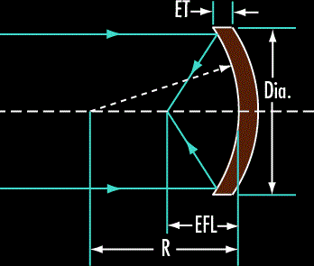
So, I am looking at the Edmund Optics 25mm Dia. x 50mm FL Protected Aluminum, Concave Mirror Stock No. #43-466 priced at $37.50ea for the collimating mirror and the imaging mirror.
- Diameter (mm): 25mm
- Effective Focal Length EFL (mm): 50
- Radius (mm): 100
- Edge Thickness ET (mm): 3.00
And the Edmund Optics 1200 Grooves/mm, 25mm Square, VIS Holographic Grating Stock No. #43-216 priced at $135.00 for my grating surface.
- Dimensions (mm): 25x25
- Groove Density (grooves/mm): 1200.00
- Thickness (mm): 9.5

Where these are not what a lot of people consider 'cheap'... they are as far as this stuff goes.. It's actually cheaper than anything I could find on eBay....used.

Discussions
Become a Hackaday.io Member
Create an account to leave a comment. Already have an account? Log In.
Thanks for the info!!
Are you sure? yes | no
Are you sure? yes | no
Are you sure? yes | no