After turning it on and off many times I noticed it was always failing on the same external memory test number: 10.. What did 10 mean...
My external memory test routine is very simple, it writes an incrementing number (starting at 1) to the external memory addresses 0x200 to 0x2ff. Then it reads them all back, if it reads back the same numbers it wrote then it assumes success.
10 means it successfully read back 0x200 through 0x208 (values 1 through 9) and then failed at 0x209. 0x209 in address lines is 10 0000 1001 meaning A0, A3, and A9 are hot. The value 10 in data lines is 1010 meaning D1 and D3 are in use.
So I started down the path of verifying the ratlines and solder points for these were all valid. They were, but in my experimenting I discovered I wasn't getting consistent resistance readings (using my multimeter) with D4 and D7. I tried for quite awhile to reconcile this with my expected D1, D3, A0, or A3 being bad - but I couldn't come up with any logical reason.
Then I decided to remove the Professor (ATMega chip) and make sure the solder points on the bottom of the PCB went all the way up to the socket we soldered to the board. Again, that was fine.
However, when reseating the Professor I noticed some of the legs didn't seem quite right...like maybe they bent at an angle and didn't go through the socket (I should have taken a pic). So I took great care to straighten them all again with needle nose pliers and tada!, it all worked!!! The ATMega shares address and data lines on the same pins - so I'm guessing some of them were bent and never made it in the socket correctly.
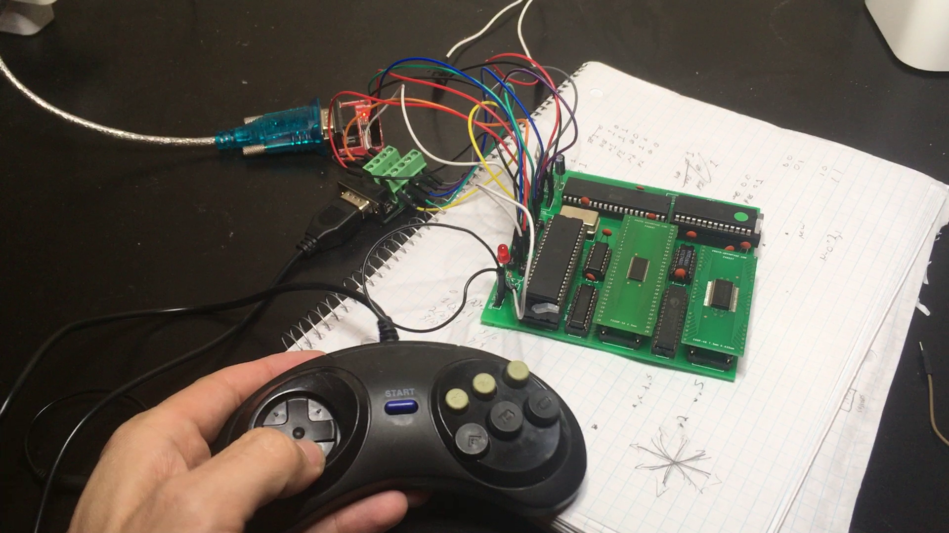
Here's me testing it out...notice I'm pressing down on the D-Pad
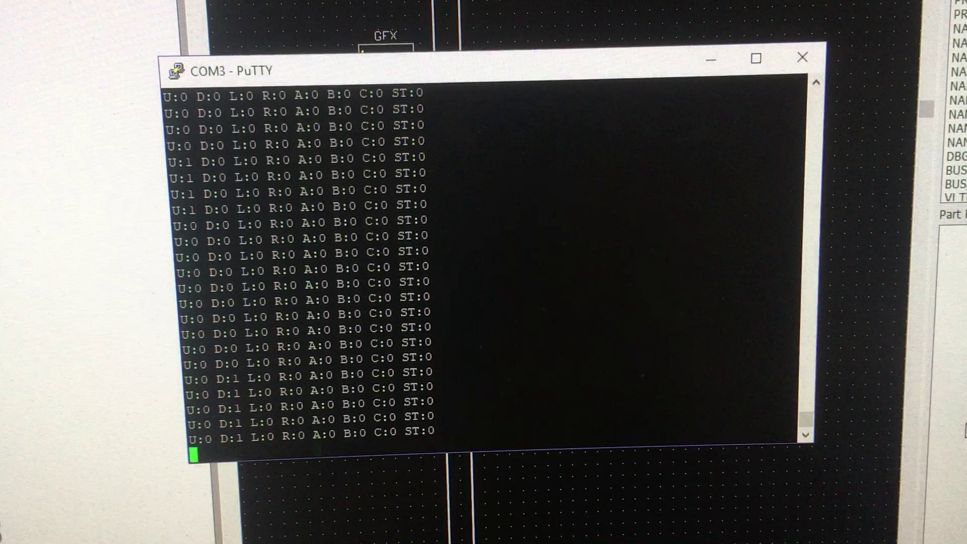
Here is the serial terminal app (Putty) reporting it correctly! (The D for Down is at 1):
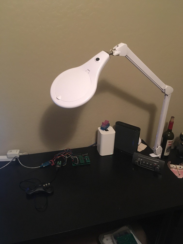
btw - a quick side note, I ordered this awesome LED soldering light / magnifying glass off of Amazon, it made checking the soldering points much easier! https://www.amazon.com/gp/product/B010TOTT58/ref=oh_aui_detailpage_o00_s00?ie=UTF8&psc=1
Next up is to get the real IO connectors soldered on for the joypad, serial out, and gfx expansion.. then I'll switch gears and start working on the graphics board!
Discussions
Become a Hackaday.io Member
Create an account to leave a comment. Already have an account? Log In.