Having a look around for layout recommendations initially chips like MAX4196, MAX1452 and MAX1455 cropped up - preamp and signal conditioner ICs for strain gauge measurements. But that's a bit beside the point so here's just a reference for further reading.
https://www.maximintegrated.com/en/app-notes/index.mvp/id/1069
More intriguingly there's ADS1231 for ten times the price of an HX711. Check out its features:
- 24 bit 3rd order ratiometric sigma-delta ADC , 4th order sinc filter
- 10 SPS / 80 SPS with 50 / 60 Hz and harmonic suppression
- 128x gain (20mV FS, AVDD up to 5V)
- 2-wire SPI-ish synchronous interface (SCLK, DOUT)
- "no register progamming"
- sleep mode induced by keeping SCLK high
- internal oscillator and external clock input option
http://www.ti.com/lit/ds/symlink/ads1231.pdf
ftp://ftp.ti.com/pub/data_acquisition/ADS1x31REF/
https://www.mouser.com/ds/2/813/hx711_english-1022875.pdf
While HX711 provides the same features (except the datasheet doesn't go into detail as to how the 50 / 60 Hz suppression is implemented, possibly due to patent issues) - it expands the capabilities by adding an input multiplexer with different gain options, a bit-counting command decoder for the new config options and sadly eliminates both the filter / bw limit capacitor after the PGA stage as well as the differential reference input.
ADS1231 relies on an external voltage reference and implements sleep mode with a low side switch while HX711 has an integrated LDO with external PNP pass transistor and its power-down capability.
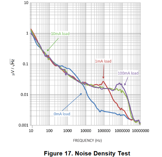
general LDO noise
Since we're talking 20-100 nV precision it's very interesting to see this seeming neglect of differential reference implementation in the HX711 design. ADS1231 design choices also seem to hint at a possibility that integrated LDOs are usually not good enough - even dedicated external "ultra low noise" LDOs like http://www.ti.com/lit/ds/symlink/lp5907.pdf still feature 10µVrms (10 Hz .. 100 kHz BW, *with* 1µF output capacitance?) with a substantial 1/f-noise contribution in the 10-100 Hz band
 This leads to suspect that just hooking up excitation and AVDD to some LDO will in both cases not be enough for proper performance. Capacitors themselves contribute some noise (kTC noise https://en.wikipedia.org/wiki/Johnson%E2%80%93Nyquist_noise#Thermal_noise_on_capacitors ) and depending upon the dielectric possibly some piezoelectric noise as well (hopefully no pyroelectric effects though), but bigger is essentially better here, as long as the LDO doesn't go unstable.
LDO stability has to be ensured via output capacitor selection - both capacitance and ESR must be in a certain range and the input capacitor should match the output capacitor by some factor (stick to typical ratio from datasheet). Larger capacitors can be added when they are decoupled with R or L elements but resistors will again contribute some noise ( https://daycounter.com/Calculators/Thermal-Noise-Calculator.phtml : 5.185k: 346 nV vs. 667R: 117 nV) - and regulation and bandwidth are not preserved. When using inductors, resonances have to be controlled by adding RC series elements. Implementing an RC pi filter is very similar to adding an output resistor to an opamp to re-establish stability in capacitive loading scenarios.
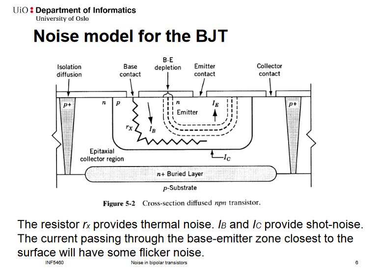
BJT noise considerations for HX711
According to
http://www.analog.com/media/en/Other/Miscellaneous/PM_ldo_design_08451b.pdf
the primary noise source of an LDO is its reference, so proper bypassing of the voltage reference pin might be just as effective as increasing the LDO output capacitance. This is particularly relevant for HX711.
As for the PNP transistor...

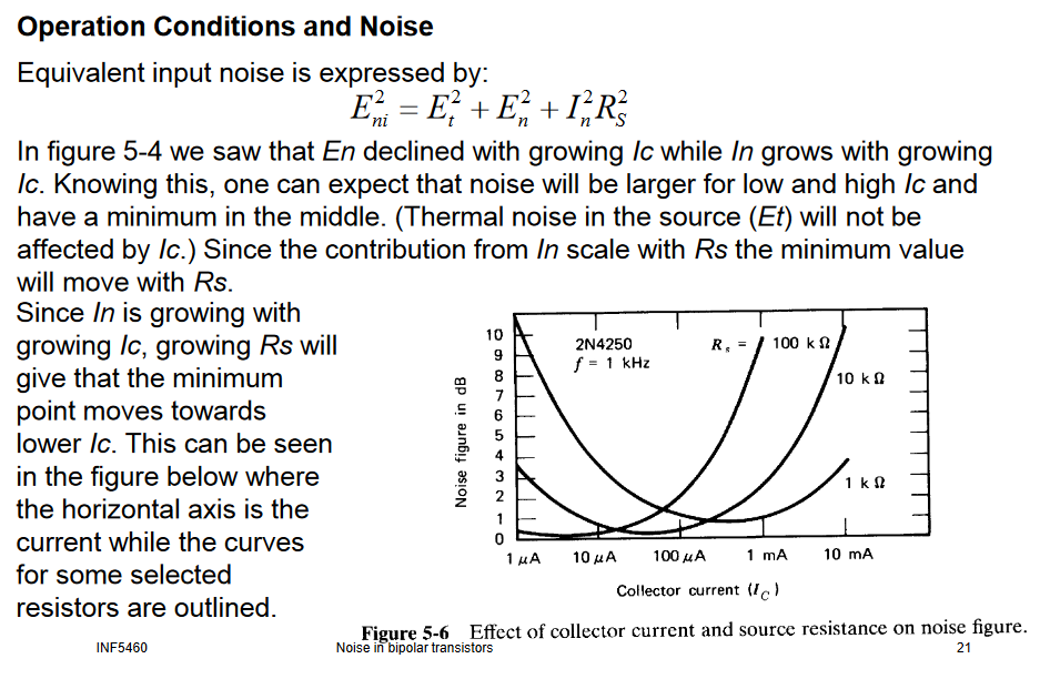
Obviously a moderate collector current can sometimes improve the noise figure (how much SNR is degraded when the transistor is used as an amplifier)
https://leachlegacy.ece.gatech.edu/ece6416/f09/ece6416_f09_exp04.pdf
https://www.allaboutcircuits.com/textbook/semiconductors/chpt-4/bjt-quirks/
Action plan?
- ADC supply input filtering, ferrite beads, proper grounding scheme (inspect ADS1231 reference design)
- select high current gain transistor, esp. at the ~mA operating point of the load cell excitation, keep in mind one can also parallel transistors in an effort to change the noise figure?
- proper bypass capacitor for the LDO reference (100 nF C0G || 4.7µF X7R with 2-5x voltage rating of the operating voltage), read http://www.ti.com/lit/an/slyt489/slyt489.pdf
- filter between LDO and excitation / AVDD input
- allow multiple samples for ADC to settle
- check susceptibility to temperature differentials (in that regard maybe also not having the LDO power transistor onboard the ADC chip has its benefits)
a quick chat with a mixed signal ASIC designer
Some recollections from a discussion with a chip designer.
There seem to be some intricacies that determine design decisions. It would be really interesting to figure out the process in which HX711 is being produced. It ought to be easy to implement the 24bit ADC and integrate the LDO on the same die when using a BiCMOS process and proper guarding (gory details see http://www.iue.tuwien.ac.at/phd/puchner/node48_app.html ) whereas other less evolved semiconductor processes will not allow this degree of mixed signal and power integration. The supply voltage range of up to 5.5V is a hint, but not definitive.
Regardless the technology it always requires critical assessment whether it is allowed to place a heat source on the chip, causing analog circuitry parts to drift around as the device parameters and operating points of individual transistors change. So offloading the LDO power stage might be more beneficial than going for more complete integration.
It may well be that ADS1231 achieves superior performance by using a fully differential ADC architecture. Once more it feels like the HX711 designers made a few daring simplifications. A test to expose the quality of the ADC would be to assess integral non-linearity over the input range - ADS1231 is specified to deliver +/- 8ppm INL while neither "INL" nor "linear" are mentioned in the HX711 datasheet.
Depending on how the VFB input stage is implemented (e.g. CMOS gate) the feedback divider impedance, being the source impedance to that pin, may affect the regulator noise characteristics. HX711.VFB input current is not specified and needs to be measured to clarify.
Everything below 120 dB common mode rejection is not so great - and HX711 is only quoted to have around 100 dB, with no mention of frequency or bandwidth. This suggests improvements are possible by connecting DVDD straight to 5V or another 3.3V rail, passing filtered 5V to an LDO with good supply ripple rejection, dropping down by 0.5 .. 1 V and dropping yet again to 3.0-3.5V for strain gauge excitation.
Input CMRR would also need some help by adding proper combined common mode and differential mode filtering.
To keep things simple and acknowledge part variations in cheap capacitors, the differential mode input capacitor should be significantly ( say 2 orders of magnitude) larger than the common-mode caps (think 2x 1..10 nF w.r.t. 1 µF differential mode).
kTR noise of the voltage divider should be a minor contribution to regulator noise but it still provides a means to adjust the DC current through the pass transistor if there is still some room for noise figure improvement.
final thoughts.
The few simple things I could add to it thus far would be that it might also be worthwhile to add series termination resistors to the digital lines - or even a quad resistor array with RC T-filters to control slew rates and at least test the internal RC oscillator vs. an external precision clock source.. or maybe even add some jitter for testing purposes.
The worst thing about HX711 might ultimately be its input offset drift of 200 µV at x128 gain. Hey, it has a secondary input which might be using the same gain stage! (not with full conviction because gain options for the two inputs are mutually exclusive). Maybe connecting input B pins via resistors to VBG (which is within the valid CM voltage band) might serve to measure the input offset observed after the muxer?
ps.
forget what I suggested about input B being connected to VBG. If the offset voltage is the same (proportionally) it would make a lot more sense to hook input B up to input A with INP and INN reversed.
Yet another way would be to use a SPDT or DPDT IC like DIO3712LP10 to reverse the differential mode component of the sense signal by flipping excitation polarity. Still cheaper than an HX712 ignoring availability issues :)
 helge
helge
Discussions
Become a Hackaday.io Member
Create an account to leave a comment. Already have an account? Log In.