 helge
helgeIntroduction
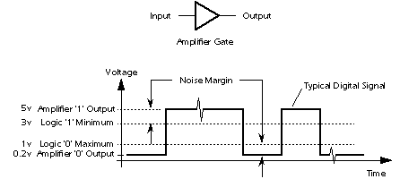
There's a lot of room for paranoia when stepping from the digital domain with its noise margins, supply ripple and voltage tolerances into areas of analog and mixed signal circuitry.
Connectors, analog switches, scaling networks, voltage reference and supply filtering components are situated in the analog domain while dedicated ADCs and controllers with integrated multiplexers, programmable gain amplifiers and ultimately ADCs are mixed-signal ICs.
Suddenly there are concerns about internal electromagnetic compatibility, identification of sources of - and ways to mitigate - interference. There are also selected aspects of systematic measurement errors which will not be discussed in this log (temperature effects like bias current / voltage shifts, reference voltage drift, thermoelectric voltages; mechanical effects like strain hardening, yielding or just creep, hysteresis of sensing elements, non-ideality of summed sensing elements and so on).
There are a few coupling mechanisms for EMI to consider when creating a new layout or fixing an existing one.
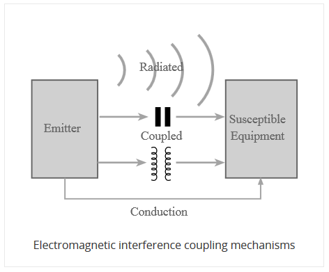
Obviously the effects - noise currents into or noise voltages added to analog nodes of the circuit (including supply rails) - are the same no matter the way they were created. The above nomenclature helps pointing at the causes of interference while looking at the interaction of electric and magnetic fields yields ideas how to address susceptibility.
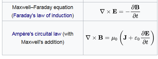
A brief detour through classic electromagnetism.
Furthermore it feels to me like the distinction between "coupled" and "radiated" EMI often doesn't make a lot of sense at the component or PCB trace level.
If part of the circuit picks up interference, it's susceptible to the local values of the electric or magnetic fields while "radiated" only suggests to me that there are electromagnetic waves involved which in turn means that one is only supposed to be concerned with field components that are able to propagate through space.
To quote https://en.wikipedia.org/wiki/Near_and_far_field on the distinction of field zones,
"Far-field E (electric) and B (magnetic) field strength decreases inversely with distance from the source, resulting in an inverse-square law for the radiated power intensity of electromagnetic radiation. By contrast, near-field E and B strength decrease more rapidly with distance: part decreases by the inverse-distance squared, the other part by an inverse cubed law, resulting in a diminished power in the parts of the electric field by an inverse fourth-power and sixth-power, respectively. The rapid drop in power contained in the near-field ensures that effects due to the near-field essentially vanish a few wavelengths away from the radiating part of the antenna."
Usually the near field is a complicated mess (topologically) but what matters is the net induced current or voltage. surfaces act as capacitors, loops and slots act as inductors which couple to alternating fields, constituting capacitive and magnetic coupling respectively.
Inversely, purely magnetic (loop antennas) or purely dielectric (DRA) structures work fine while predominantly coupling to one of the fields. The complementary field is being regenerated as per
So "just make bad antennas". Minimize susceptible loop areas, block AC magnetic flux paths by adding ground planes and if possible arrange components to they provide Faraday shielding against electric fields (e.g. stacked PCBs or dedicated shielding cans).
Even if high frequency fields are outside the frequency bands of relevance, they might still interact non-linearly with the circuit and can thus be rectified into voltage offsets or bursts. This is where the dimensions come into play, at least in the far field and without resonant coupling effects. It always helps to make circuit loops as small as possible but where traces route to other quadrants of the PCB of off-board, splitting nets (from an RF perspective) by inserting ferrite beads and blocking interference at the inputs (both power and signal) is usually a good thing as long as peak and DC current limits are observed.
Conducted EMI
That should do for non-conducted EMI. Conducted interference luckily is more of a planar circuit-level problem once trace segments, branching and planes are properly propagated back into an augmented schematic, accounting for trace resistances and inductances.
Admittedly the intuition lives off "reading" circuit layouts and assigning guesstimated sheet resistances and relative inductances.
Tools like Keysight ADS (formerly EEsof EDA) are used to bridge this valley of subjective experience with somewhat credible numerical simulation results and help with distributed PCB and circuit element modeling.
https://connectlp.keysight.com/EMOSignalIntegrityPowerIntegrityResourcesfromKeysightEEsofEDA
Identifying design goals
There are three mixed subcircuits which have to be looked at in the design at hand, on top of the PCB connections themselves. Or, In other terms, everything is relevant :)
Power, analog and digital signal connections aside (input decoupling and bypassing might be in order), an SoC ADC and the HX711 are on the receiving end of whatever comes their way from the on-board DCDC converter, power connector and transients caused by the SoC itself.
DCDC converter design will have to be covered elsewhere and the SoC ADC peripheral with rather low resolution won't be too critical (that is, offset voltages , ground connection and input noise should still be controlled to a reasonable degree while being assumed to work without extreme measures), the HX711 "+/- 20mV full scale differential input voltage" worries me a bit.
- minimize DCDC conducted EMI by proper layout design
- minimize DCDC and SoC board coupled interference by maximizing the distance between the HX711 analog part and the DCDC zone
- utilize Faraday shielding, star grounding / ground island formation
- observe distinction between analog, digital and power ground zones
- avoid groundplane slotting near the RF antenna, stitch top and bottom ground polygons with vias (fencing, sprinkling)
- stay sane
Input power filtering might be easy to do, possibly even by plementing an RC filter where R is contributed by a polyfuse to avoid the BOM cost for additional inductors.
For the time being let's assume the DCDC is carted off to a distant location, on its own patch of ground and input as well as output capacitors tied to the one point where it connects to system ground.
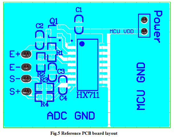
Faraday shielding is a bit of a premium feature. Assuming a continuous ground plane on the base PCB and an acceptable ground plane in the SoC board this cavity should be a good place for placing the HX711. it must be noted however that board-to-board interconnects driving fast digital signals will still act as a significant source of noise. Any unused GPIO could be made an output and driven low. Due to cost optimization, the single-sided component loading implies HX711 cannot be facing away from the DCDC and SoC board. Designing for wave soldering might remove this constraint, replacing reflow soldering and some second step to solder the connectors.
Preferably HX711 is located at the far end of the SoC board, away from the RF antenna. It is not clear to what extent the high power radiation from a wifi chip antenna will interfere with HX711 - this will have to be quantified in an actual experiment with real hardware.
experimental work
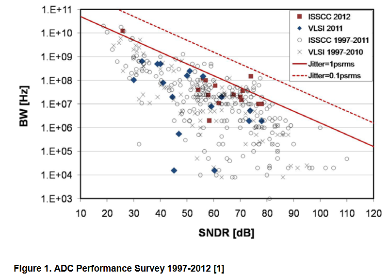
Just for the sake of completeness: (All?) ADCs are influenced by converter clock jitter and there are ultimate limits to achievable "Signal to Noise + Distortion" ratio vs. bandwidth. For the not-so-bleeding-edge HX711 the external clock option is assumed to be mostly benificial to achieving a consistent sampling rate, not to improve accurary.
http://ece.tamu.edu/~spalermo/docs/clock_jitter_effects_delta_sigma_modulators_saad_2012.pdf
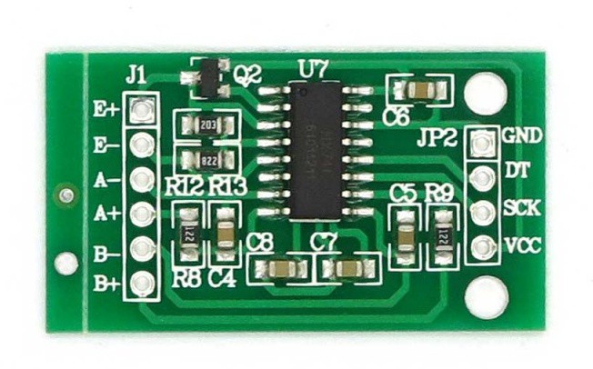
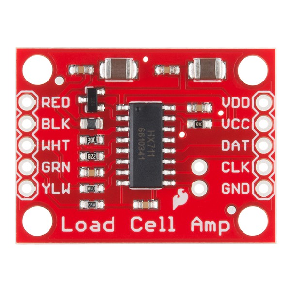
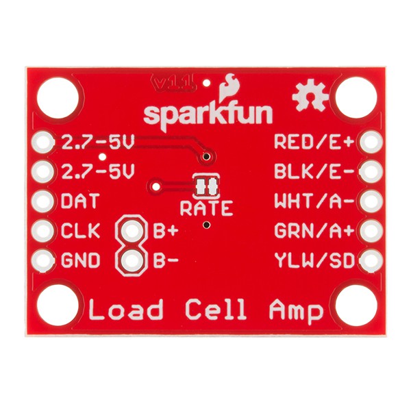
Interestingly, someone on the internets has taken it upon themselves to quantify HX711 noise free resolution and supply noise influence.
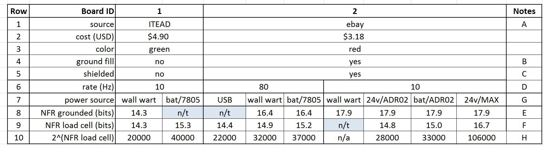
https://forum.arduino.cc/index.php?topic=365107.0
shielding has been applied after the fact and pulling both inputs to GND violates the input common-mode voltage range. Since the reference design foresees all ground connections to the analog signal ground, no distinction is made here. Keep in mind that this does not translate to being allowed to use any ground around the HX711 on a board with other circuitry.
Apart from that, there is some improvement from noisy USB to individual supply with LDO and various 5V voltage references (ADR02, MAX6350). Sadly supply noise tends to be most bothersome where LDOs fail to perform supply ripple rejection. As a general rule, both load ripple and input ripple high frequency components should be isolated from an LDO via passive filtering (de-Q-ed LC filters). Switch-mode power supplies should also be decoupled with a common-mode filter at the input.
My bet is on LC or RC input filtering without an additional LDO.
There are two more things to consider.
The red PCB has this weird ferrite bead arrangement which might prove performance. Additionally S8550 seems rather mediocre compared to other PNPs with higher beta and lower capacitances which may give rise to greater regulator noise.
I'd try direct connection of the pass transistor to a bypass capacitor, feeding into an RC pi filter made with a nice metal film resistor. The ADC is referenced to the same excitation voltage to compensate for scaling errors but I cannot make recommendations to which side of the filter to best connect it. Solder jumpers on early revision PCBs, go figure :)
To summarize: LDOs are not the answer, but proper supply and analog reference filtering should bring good improvements. Do use a nice patch of ground for HX711 alone and at least try to avoid capacitive coupling to noisy nets as well as magnetic coupling of DCDC stray fields.
Do test 2.4 GHz interference effects.
re ground fill:
Input filtering.
While the designers of of the red PCB at least made some effort to implement input filtering, those of the green one couldn't even be bothered to implement a proper differential mode RC filter, causing a mixing of differential and common mode components at the ADC. This is what a differential input RC filter should look like (equations see link)
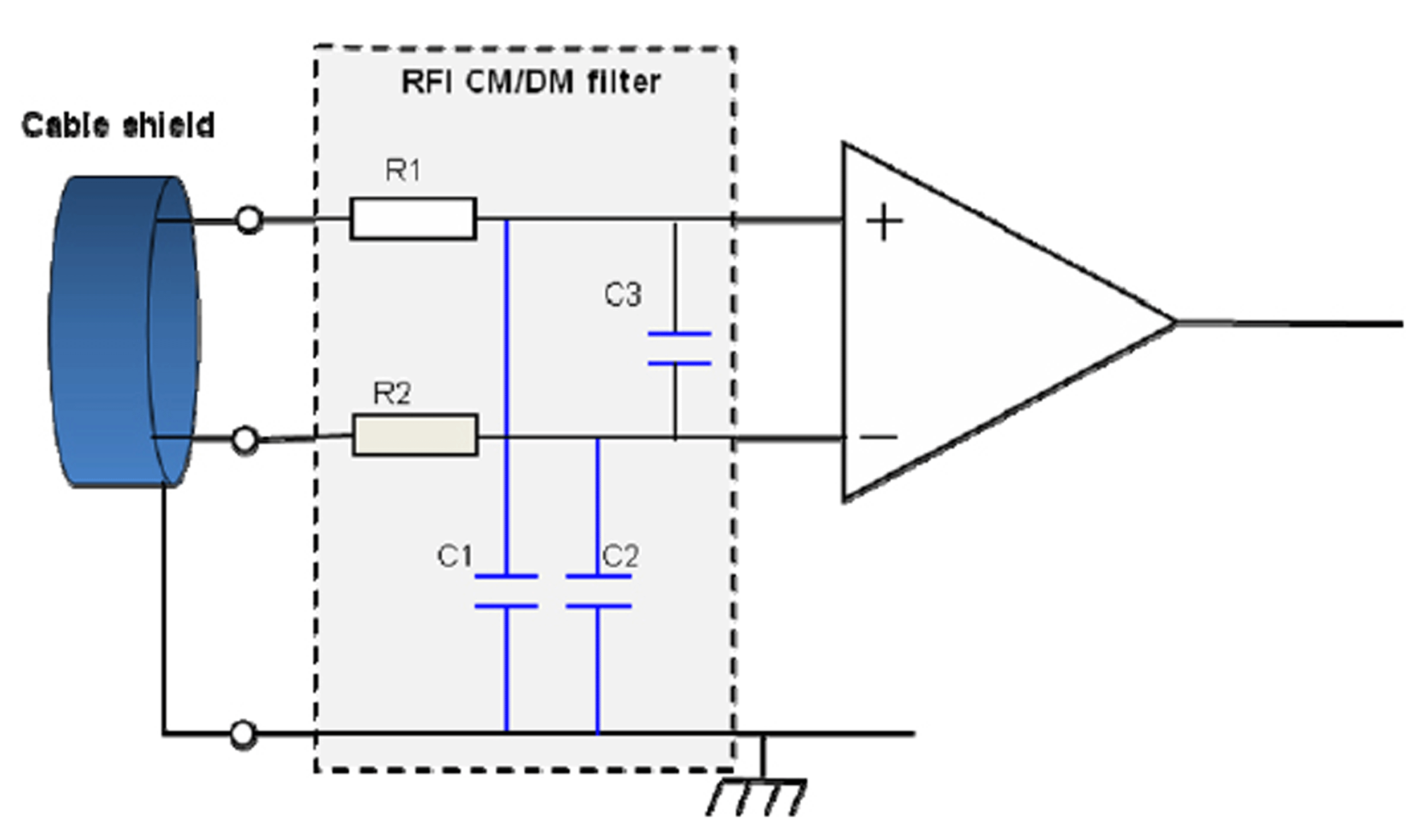
https://www.eetimes.com/document.asp?doc_id=1272503
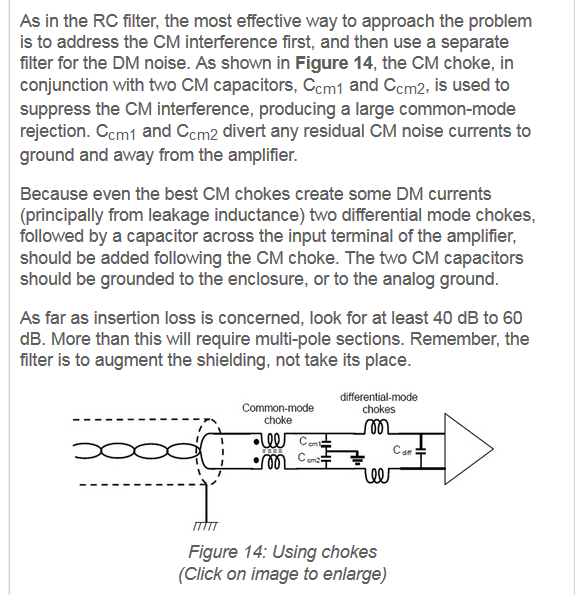
Re power supply CM + DM filtering
don't use rod ferrites (aka "EMI cannons"), they do pick up a lot of junk from the surroundings while radiating like mad when tasked with filtering supply ripple. single layer wound toroids (WE makes some nice ones).
 https://www.vkham.com/Info/ferro/tut_5a.html
back to layout design, until next time.
-
further references:
https://pdfserv.maximintegrated.com/en/an/AN5100.pdf
https://www.mikrocontroller.net/topic/415004
http://www.ti.com/lit/an/slyt202/slyt202.pdf
https://electrooptical.net/static/oldsite/www/frontends/frontends.pdf
Discussions
Become a Hackaday.io Member
Create an account to leave a comment. Already have an account? Log In.