 Ryan Logsdon
A step-by-step guide, using KiCad to make a simple breakout board for tiny, tiny chips!
This is part 2: creating the physical component layout.
1.
Open the EESchematic ("Electronic Schematic Editor")
2.
Import Our "Part 1" Tutorial Work
Now that we've created a logical chip, we can import it into KiCad.
Preferences > component libraries > add > (find your newly saved file) > ok
3.
Place the Component on the Board
Place (as in File/Edit/View/.../Place) > Component > (type your component's name in the filter) > select the component > ok
4.
Working with the Footprint
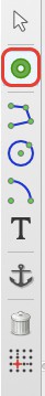
Select the Footprint Editor icon

File > New Footprint > (add a name) > ok
5.
Change the Default Text
Change "REF**" to "U**"
6.
Add a Pad
Add a pad to your footprint. Drop it in place anywhere.
Right-click > Edit Pad > (change "Pad type" to "SMD" & change "Shape" to Rectangular").
7.
Add Remaining Physical Parts
8.
Creating a Library
Click the "Create new library & save current footprint" icon

Name the library "smd_MyProjectName" > ok
9.
Add this Library to Project
Preferences > Footprint Libraries Wizard > Add (choose your "smd_MyProjectName" path > ok (note that the file was saved as a *.pretty file) > next > (select "global" if in doubt) > finish
Select "Active Library"
10.
Save Footprint
Select the "Save footprint in active library" icon

Discussions
Become a Hackaday.io Member
Create an account to leave a comment. Already have an account? Log In.