 Al Williams
When you were a kid, did you ever see one of those 100-in-1 electronic kits? These were a board with a bunch of parts on them and some kind of solderless terminal. If you hooked wires up one way it was a car alarm. If you hooked it up another way it was a metal detector. A third way made an AM radio.
That's a lot like what an FPGA is. There are a bunch of blocks of functions waiting for you to wire them up. Usually, most of the blocks are exactly the same and there will just be a few special blocks, although some FPGAs will have a significant number of different block types. Exactly what each of these blocks do depends on the FPGA but luckily the tools shield us from most of this complexity. For example, there might be a block that is a look up table (LUT) that holds a truth table that converts, say, 4 inputs to 1 output. That LUT might be grouped together with a flip flop or two and some programmable inverters. Other blocks might provide RAM memory, DSP functions, or clock generation circuits. But almost always the tools will take your Verilog and figure out how to wire up the blocks to build your circuit. As an example, here's a typical FPGA cell:
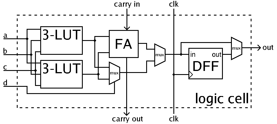
The LUTs are look up tables with 3 inputs. The FA is a full binary adder (just like the one we are using in this bootcamp, except it takes a carry in as well as an A and B input). The muxes are electronic switches. The output can be either of the two inputs based on either an input (like d for the leftmost mux) or by configuration for the other two muxes. The block marked DFF is a flip flop and we'll talk about those more in a future bootcamp.
So if you had this cell and our Verilog from this bootcamp, the tool would probably route a and b to our A and B inputs. It should be smart enough to make the LUTs just forward those bits to the full adder. The output of the full adder would route through both muxes to the output. And the carry out would be routed to our other output.
It is interesting that fundamentally an FPGA is a memory device. Instead of storing numbers, though, it stores "wires" continuing the kit analogy. Some of those wires select options (like use inverted X as the first input) and some wires connect inputs to outputs. Some FPGAs are based on RAM and need to be loaded every time they power up. That load could come from a CPU or a dedicated memory chip (usually a serial EEPROM). Some devices have a configuration EEPROM onboard. You can probably load the device from a PC using the development tools, also. But if you do, remember the next power cycle won't bring back your "code" -- you'll have to program the EEPROM device for that. Looking at the figure above, each LUT has 8 bits (3 input bits can take a value from 0 to 7). The two muxes furthest to the right are configured so that's one bit each. In addition, there will be bits to select where all the pins entering or leaving the block actually go. This can vary depending on the actual FPGA, but in general all the logic can be placed on one of many local or global busses. The clock signal (clk) probably has its own busses that is separate.
Other FPGAs are based on nonvolatile memory cells. You can program these and they stick. That's handy at development time, but there is some limit to how many times you can program them, just like flash memory. That limit is pretty high though. One advantage to the FPGAs that stay programmed is they are general ready to operate immediately when the circuit powers on. If the FPGA has to read a configuration from a host computer or a EEPROM it is going to take some time and usually the I/O pins are idle during that time. You have to take care to design around this and also your design has to be able to tolerate that reset time on every power cycle (or even a reset, typically).
It is an advanced technique, but it is possible to reprogram only parts of the FPGA on the fly. For example, a system with a CPU could use an FPGA to provide many PWM outputs and DSP algorithm. However, it could also reprogram the device to replace the DSP algorithm with another without disturbing the rest of the chip. This is difficult to get working and exactly how it works -- or if it is even possible -- depends on the FPGA you are using.
Discussions
Become a Hackaday.io Member
Create an account to leave a comment. Already have an account? Log In.