 Frederic L
I had a few hours to spare yesterday, so I pulled out my multimeter and started figuring out the board layout (reverse engineering to sound fancy). I won't go over the matrix layout as it has been covered in a previous log, but I will describe the top part of the front and back board and my findings regarding the pins of the two connectors. Here is a global view of the front and back top part.
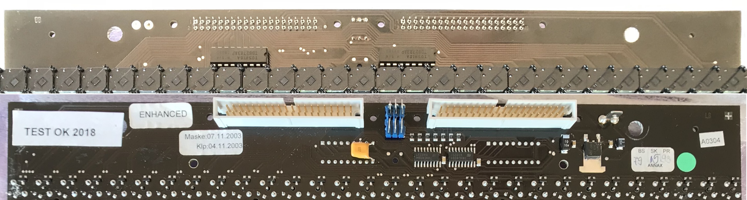
There isn't much to it, and you'll see that the few ICs on there are for driving the LEDs only. The flip dots on the other hand, are connected to the pins of the two connectors at the very top.
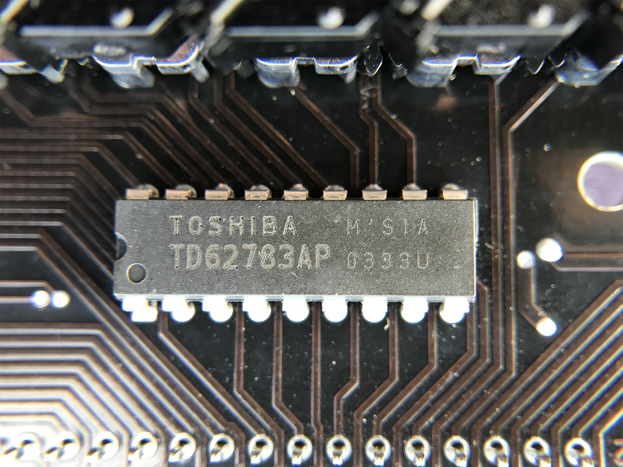
The front part is pretty empty, and not much to say besides the two TOSHIBA TD62783AP 8 Channels Source Driver.
These will source current for the LEDs for all 16 (2x8) rows.
We can also notice the trace routing going from the left connector (when looking at the front of the display) to each column. This is indeed the columns lines that will either source or sink current according to whether we set or reset the pixels.
The back part is more interesting. From right to left :
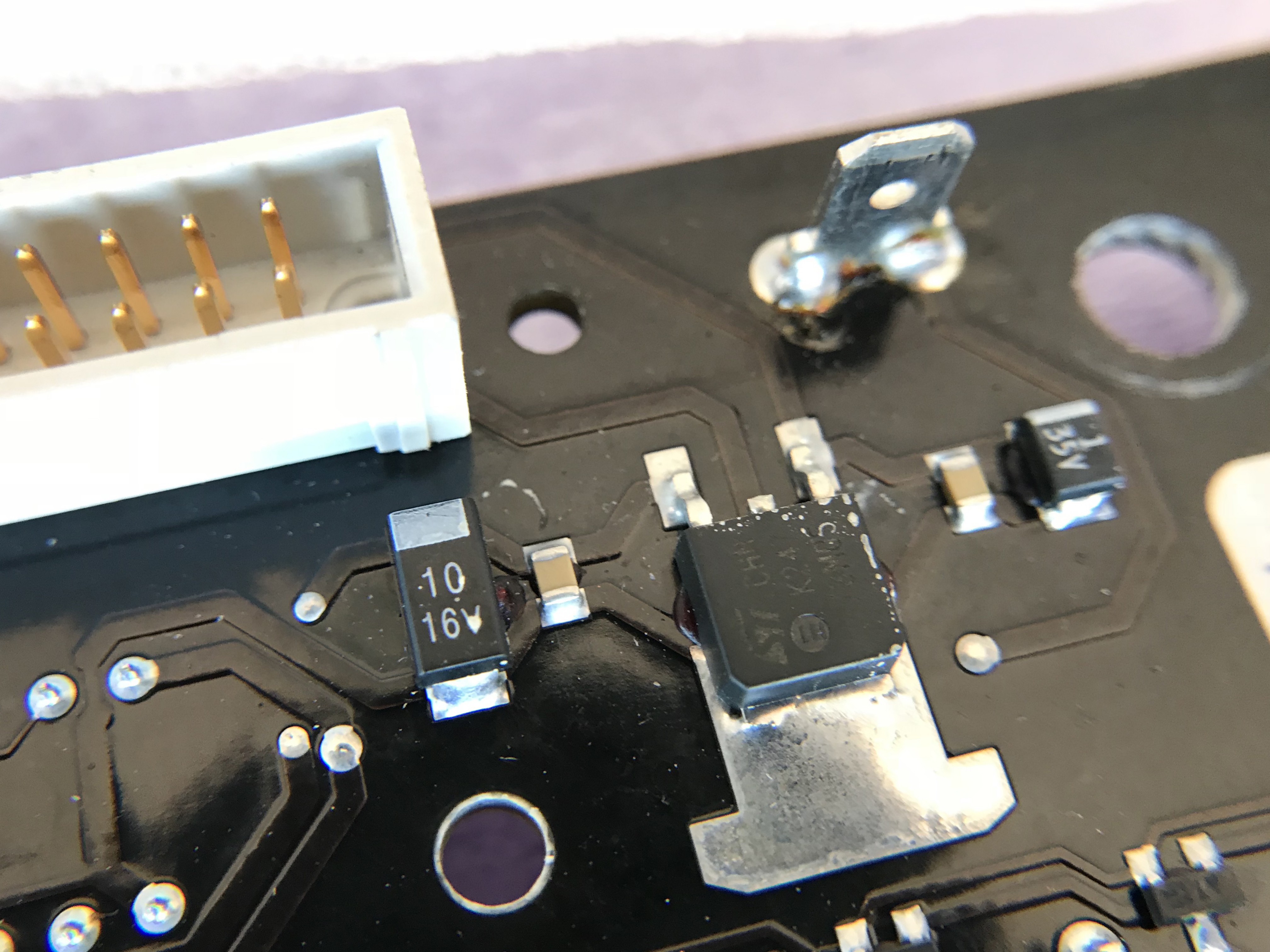
On the top right you see a tab connector. This one is for the LEDs power source, as its line goes directly to the two TD62783AP pin 9 (VCC) mentioned above.
Below it is an L78M05 voltage regulator. It takes power from the 40pin connector, regulates it to 5V and powers the other ICs on the board. The few caps around are quite common on power supplies, mainly for decoupling.
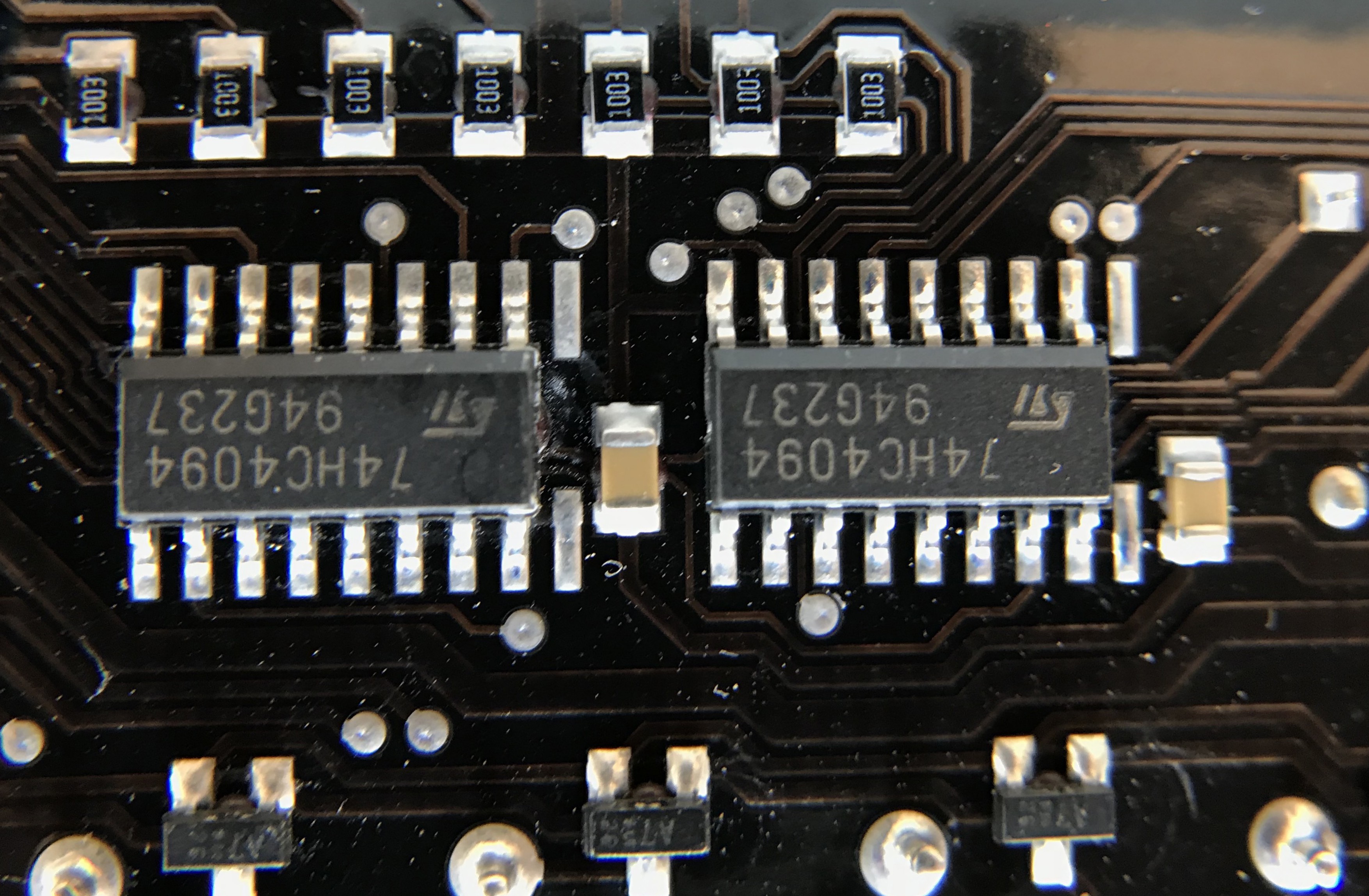
Next come the two 74HC4094 shift registers. Those are controlled from some pins on the 40 pins connectors, and their outputs go directly to the Toshiba source driver on the front. Together they control the LEDs power on each of the 16 rows.
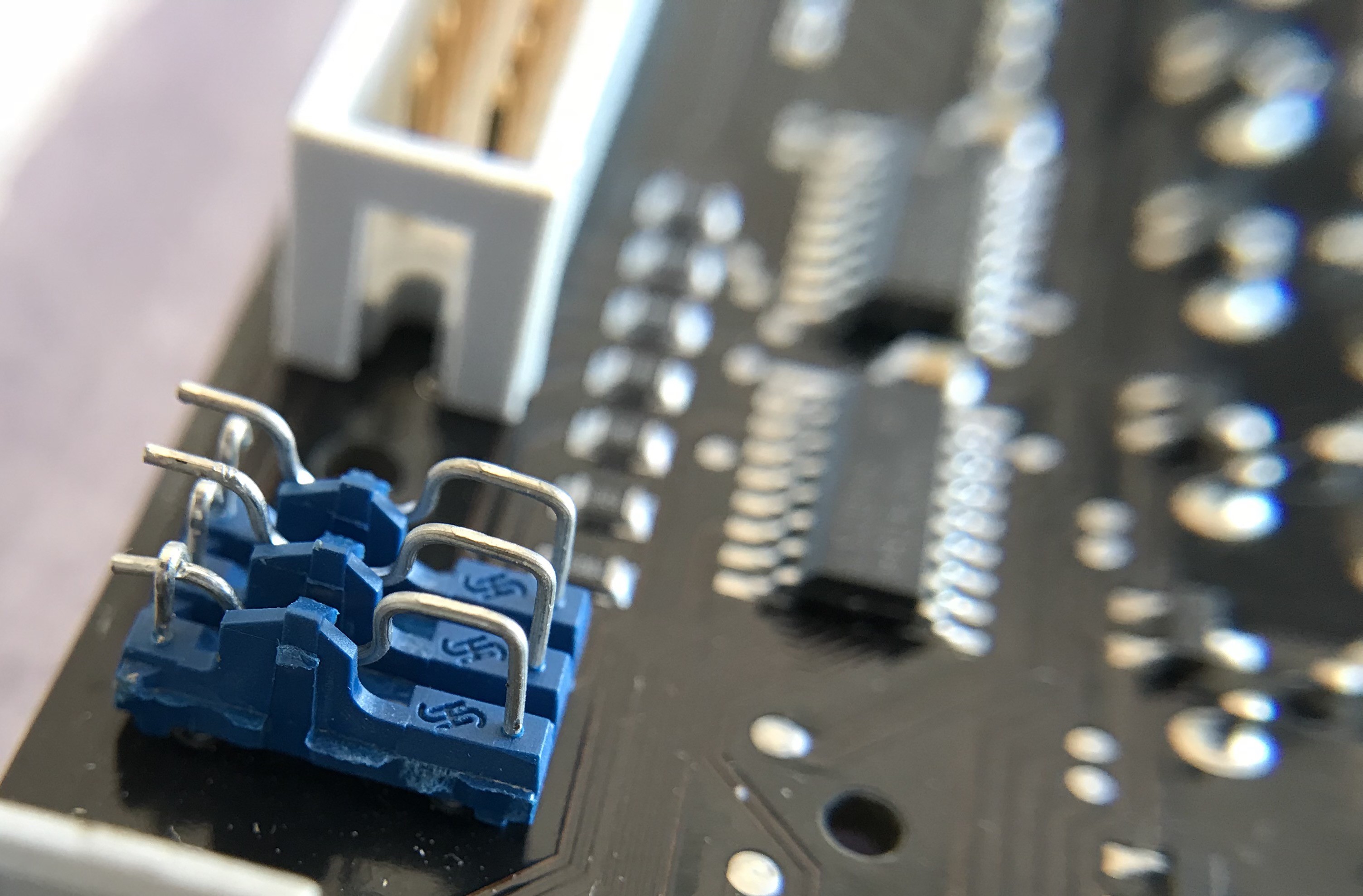
The blue thing here are three switches. On the photo you can see switch 1 is closed (the left lug goes below the hook, making contact), whereas the other two are open. Each switch connects one different pin of the 40 pin connector to the DATA (D line, PIN 2) of the first shift register (the second shift register gets it's data from the output of the first shift register. My belief here is that those switches allow to selectively control several displays LEDs with different data lines.
Finally, the most important and interesting part for the controller, are the two 0.1" pitch IDC 40-pins connectors.
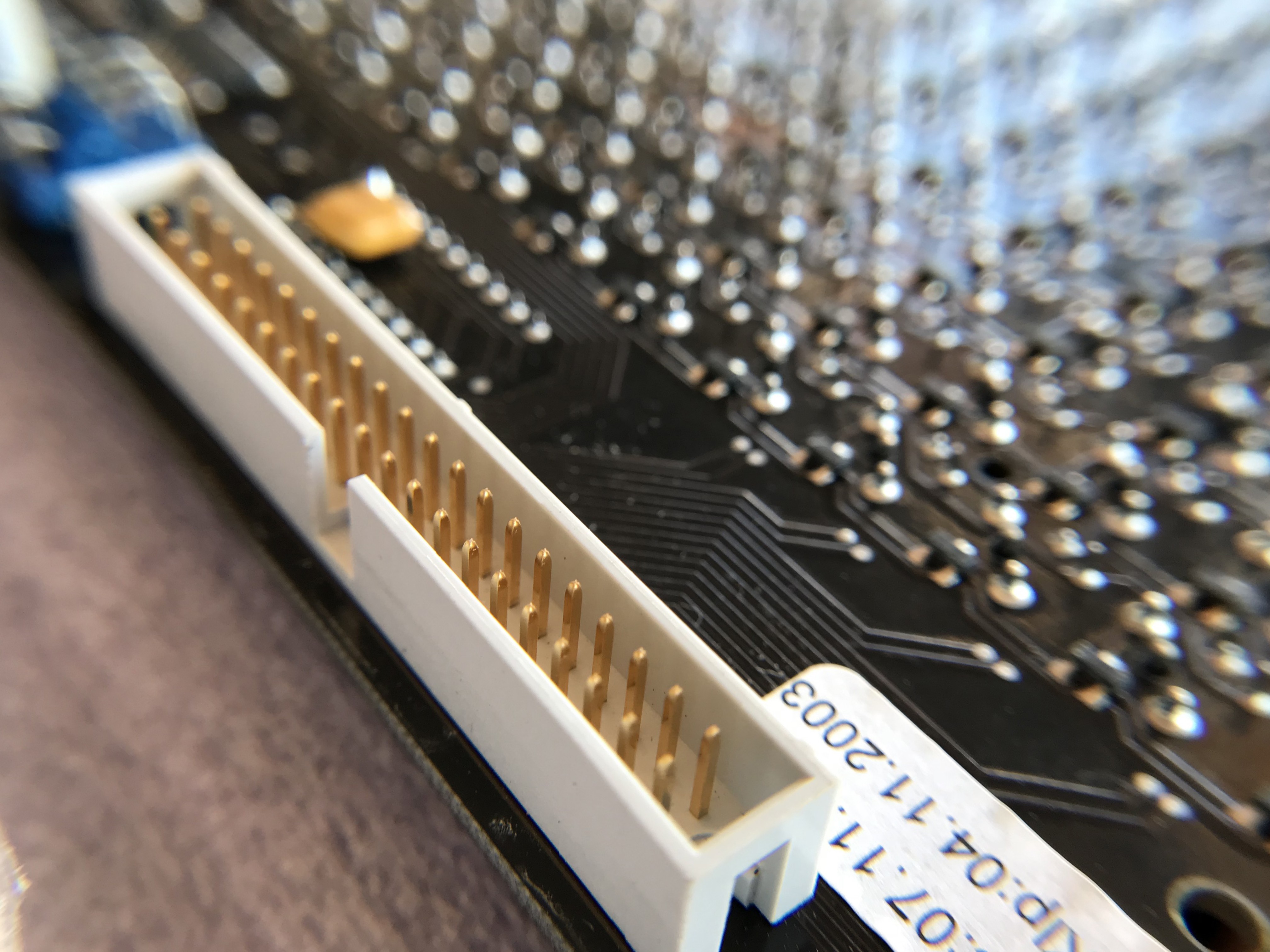
And here are what each pin is for :
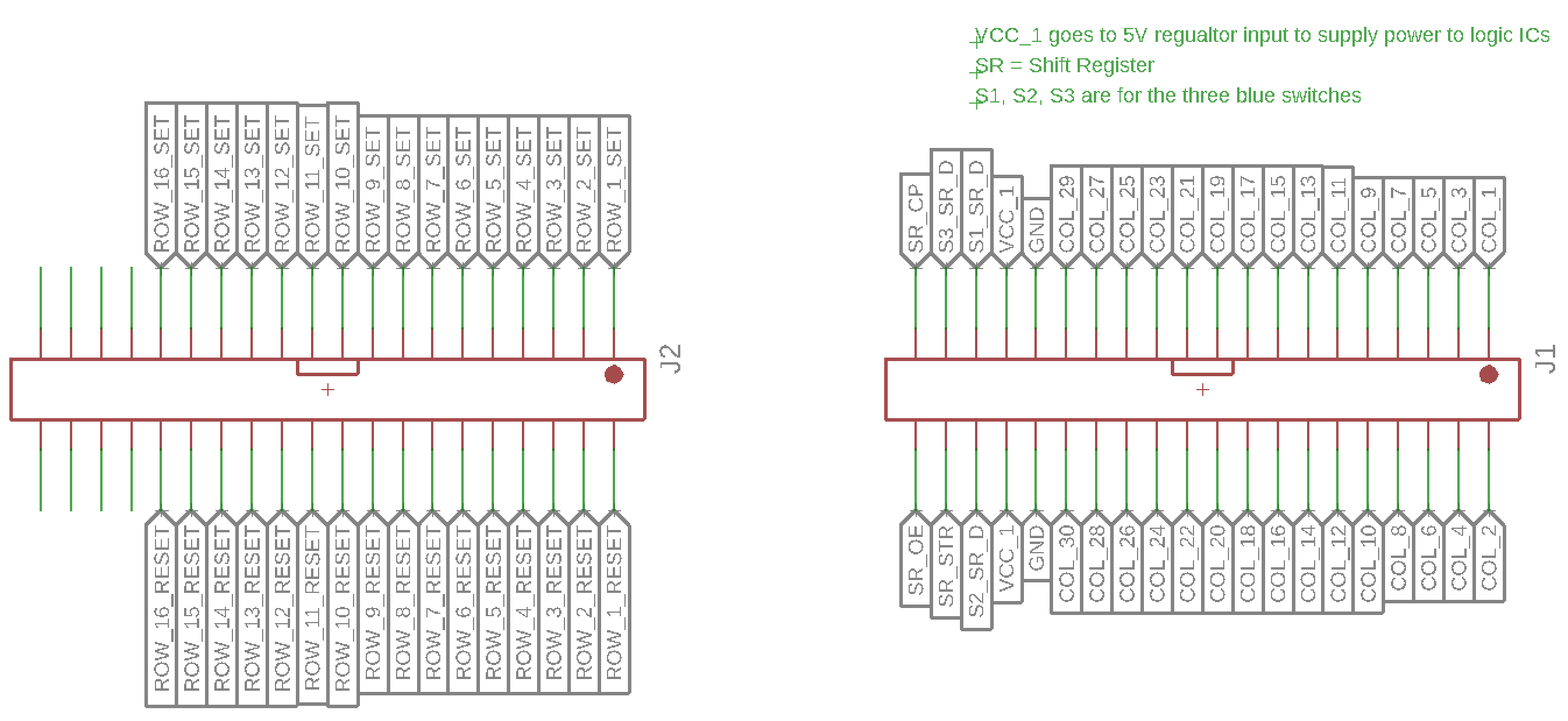
This view is as seen from the back of the board, ie. pins going towards us.
From there, let's make a controller.
Discussions
Become a Hackaday.io Member
Create an account to leave a comment. Already have an account? Log In.
Yay !
Are you sure? yes | no