Reducing noise contribution
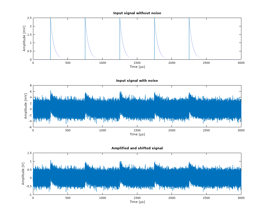
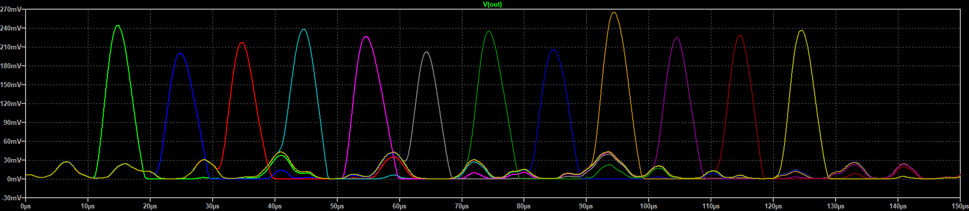
The simulations I conducted in LTSpice show that even identical current pulses yield various voltage readings. The source of this distortion is a low frequency noise originating mostly from the detecting apparatus. Most of the high frequency noise is removed by the low pass filter, but the remaining passband range is enough to introduce a significant error. Using more selective passband filter is no help as its step response shape is invalid for peak voltage acquisition.
High resolution of the detector strongly depends on the repeatability of the detecting circuitry. It provides that certain energy of captured radiation is represented by a specified voltage level. When the response varies within the span of the error introduced by noise, peaks that should represent particular isotope become blurred. Thin lines become wide enough to cover other smaller peaks and hide significant details.
There are a few ways of reducing the noise contribution:
- Lengthen the primary signal timespan by increasing feedback resistance in the TIA. With that a more selective lowpass filter can be applied and reduce the noise according to the needs. Note that this solution increases the dead time of the detector and maximum count limit, so that more active sources may saturate the detector.
- Use sensing elements with lower noise contribution and greater signal to noise ratio. In example: a photomultiplier tube with scintillator or high purity germanium or silicon detectors. In professional applications these devices are usually cooled with liquid nitrogen to really low temperatures to reduce the thermal noise to the minimum.
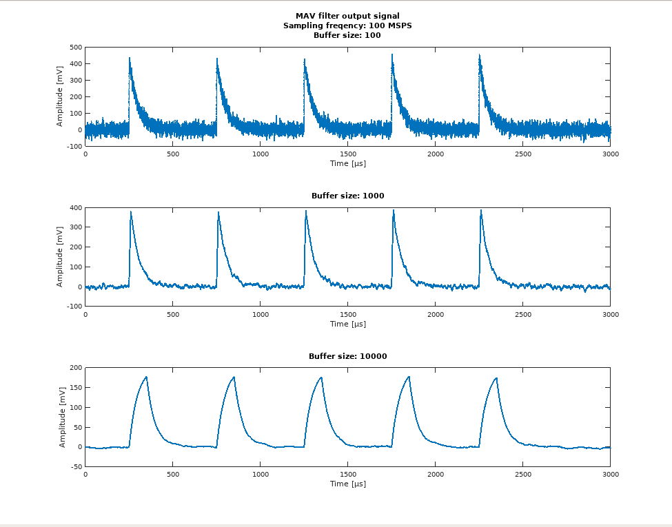
Proposed solutions either require a compromise between the parameters of the detector or are costly and out of reach. However, there is a digital filter that can tackle this kind of noise better than any of the analog kind. The best solution to the noise present at the output of the sensing element is the moving average filter (MAV). Widely described in this article: https://www.analog.com/media/en/technical-documentation/dsp-book/dsp_book_Ch15.pdf.
In short, the output signal sample is an average of all previous samples collected in a buffer of specified length. The samples are replaced subsequently by the newer ones, as the averaging window moves along.
As a result, the noise at the input of the filter is averaged to almost constant value. Depending on the length of the averaging, buffer pulses present at the input of the filter are smoothened and signal distortion is significantly reduced. Moving average filter provides greater repeatability of results at the cost of using a high-speed ADC and FPGA as a signal processing unit. On the other hand, such change enables easy alteration of signal processing path as everything can be implemented and updated in the software. I performed a few simulations with MAV to see how effective it would be. Simulations were performed using Octave, but will run with Matlab too. (available in my github repository) The signal present at the input is similar to the TIA output in the real case. With 100MSPS and a buffer of 10000 samples I was able to reduce the error to 5mV. Thinking of the third prototype there will be an additional analog output pad in case someone would like to try this approach.
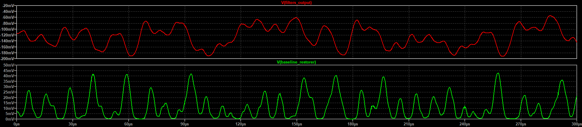
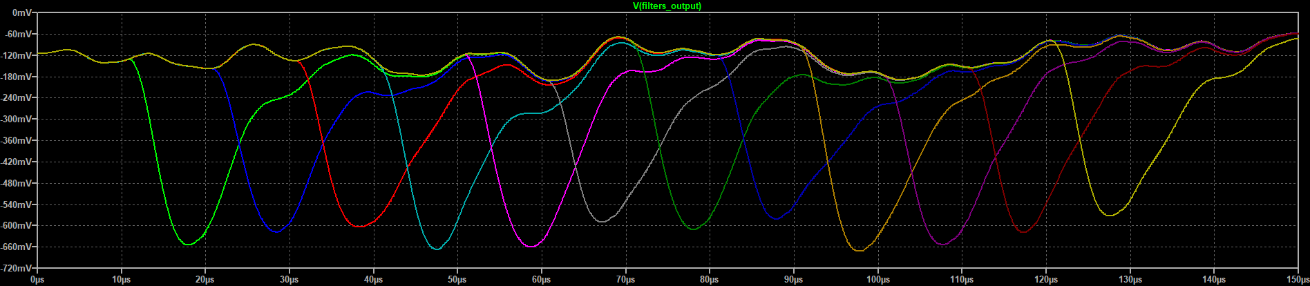
In comparison the analog filter and baseline restorer do not remove the noise too well. In the worst case the amplitude may vary even by 60mV. I hope that the spectral distribution of the noise will be a little bit different and easier to handle than a uniform one present in the simulations.
What is also interesting is that during LTspice simulations it turned out that the noise sources always have the same seed loaded. This means that the waveform of the noise signal will always be the same in each run. To see how the noise affects each peak I was forced to delay the pulse by various timespans.
Increasing sensitivity to alpha particles
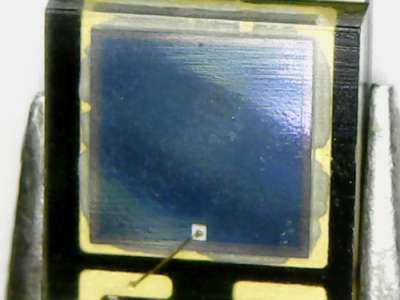
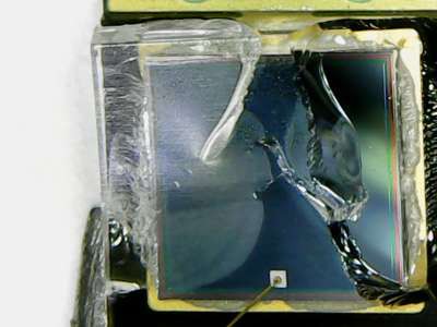
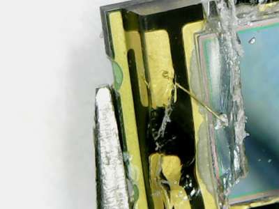
While soldering photodiodes to the board I noticed that sometimes there appeared an air bubble between the plastic case and junction. Especially in the TEMD diodes the transparent case seemed to become softer in the soldering temperatures. There were some ideas about increasing the detector sensitivity to alpha particles by sanding or milling the case untill the junction is almost exposed. Having seen that the package of TEMDs can be easily removed I prised part of the cover and investigated the bare junction. It is critical that the golden wire bonding the semiconductor plate with an electrode remains intact. Such exposed PIN diode may become useful in measuring alpha radiation, which is stopped almost by everything. In such case the detecting element cannot be separated from the source, but rather kept in an isolated environment with it.

Discussions
Become a Hackaday.io Member
Create an account to leave a comment. Already have an account? Log In.