 thomas
Oregon Museum of Science & Industry (OMSI) - giant LED wall
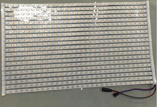
132 APA102 LED panels, 680 pixels per panel, 90,000 pixels, 300sqft, 4 Spartan 6 Mojo FPGAs
Source files on github
LED Wall at Oregon Museum of Science: https://photos.app.goo.gl/8hZoa7y9F9Lsg7Md9 (animation credit to yassi @ openprocessing.org)
The creative director wanted to put the LED display behind a wood grain pattern similar to the wall at Microsoft HQ. When the LEDs are off the visitor sees a seemless, unobtrusive wall. To make the LEDs pop behind the wood grain graphic we used a very brigtht APA102.
The resolution is about 24' wide by 14' high. That's 408 pixels wide 220 pixels tall. Not quite VGA.
The FPGA's boards are Spartan 6 on a Mojo development platform: https://alchitry.com/ The wall is broken down into 4 sections for 4 Mojo's and each Mojo receives the same HDMI signal but only grabs pixels for the section of LEDs it controls.

Alchitry has an HDMI shield for the Mojo and the FPGA code is written in their programming environment in Lucid a form of Verilog. It's great for beginners. This was my first FPGA project.
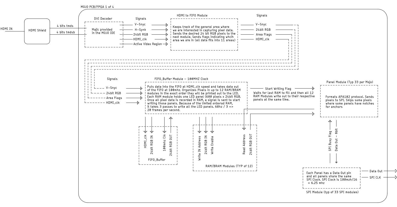
The HDMI signal is decoded and pixels arranged for each panel in local memory (RAM). There is just enough memory to save about 30% of the pixels so it takes 3 passes to arrange and output all the pixels... 60HZ / 3 gives us 20 frames per second. Thanks to David Hulton and Devin Boyer for sharing their mad FPGA memory tricks at Toorcamp 2018.
The SPI clock speed for writing to the APA102 also has speed limits as we 'race the beam.' Here's a great article by Paul Stoffregen (teensy) on these limits. The gist is the clock signals start to deteriorate between the pixels. For the 680 LEDs in our panel, I was able to write confidently at 6.25 MHZ. You can see how this clock signal is generated in any one of the 32 SPI modules in the source file under Mojo.

The FPGA generates an SPI clock and data signal to each LED panel. The signals are immediately fed from a simple shield to another custom PCB with RS485 transmitters shown above. The transmitter chips output differential signal pairs that pass easily in ethernet cords over 20-30 feet to each panel location. At the LED panel, the signals are received with transceiver chips back into clock and data lines and connected to their respective LED panel. This custom PCB also has a small DC-DC voltage transformers that take a 45VDC buss down to the 5V required for the LEDs. The below PCB has tranceiver chips and three DC-DC transformers serving 3 LED panels. Thanks to the hardware maverick Tom Moxon with Pattern Agents for help designing this circuit.

The led panels themselves are little more than strip LEDs that have been connected together. We had them customized for our particular geometry by our favorite supplier Raywu.
Mojo HDMI Shield: https://embeddedmicro.com/products/hdmi-shield
This design builds off of a lucid module example for decoding HDMI signals: https://embeddedmicro.com/blogs/tutorials/hdmi-shield-basics

Custom Circuit Boards
We used 3 types of circuit boards.
* A simple shield for the mojo that broke out all the SPI and Clock signals to the LED panels.
* A transmitter board that sends the clock and data signal out over RS485
* A receiver board that has transceiver chips, takes the signals
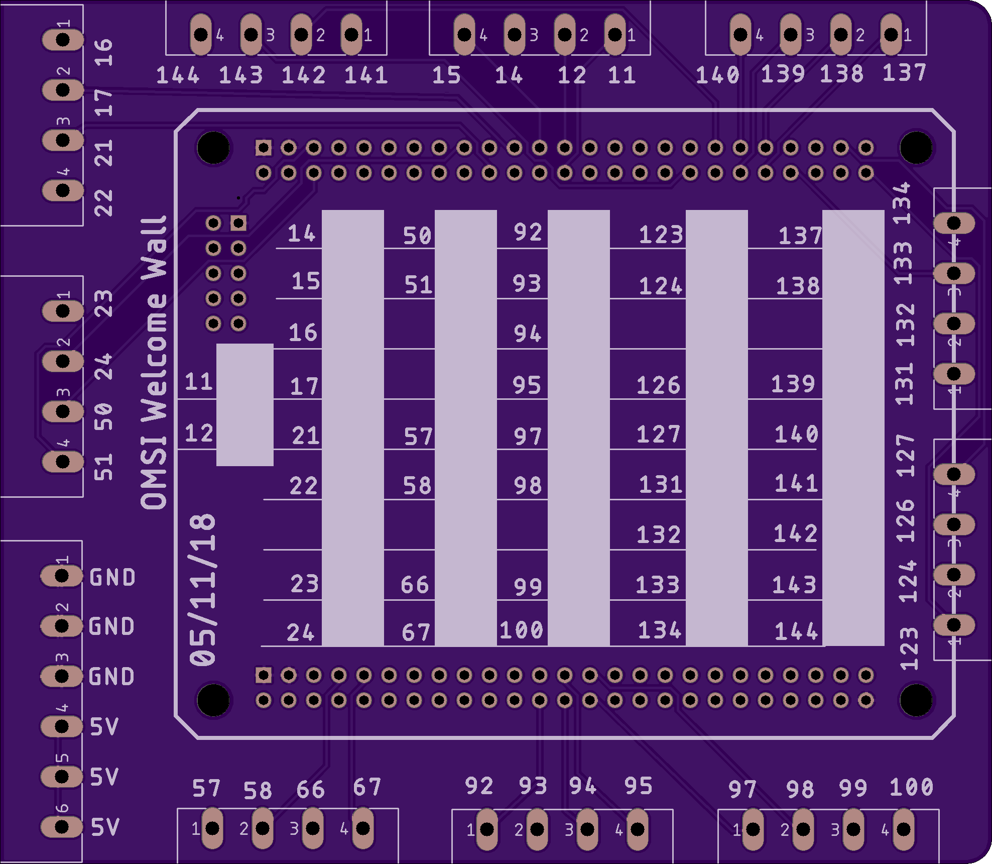
Mojo Shield has all the pins broken out. We needed 33 SPI Data pins and the clock pin was shared across all the Panels. The pins are broken out to 5.08mm phoenix connectors. The HDMI shield fits on the Mojo and this shield connects ontop of the HDMI shield. Oshpark boards here. See github for source files.
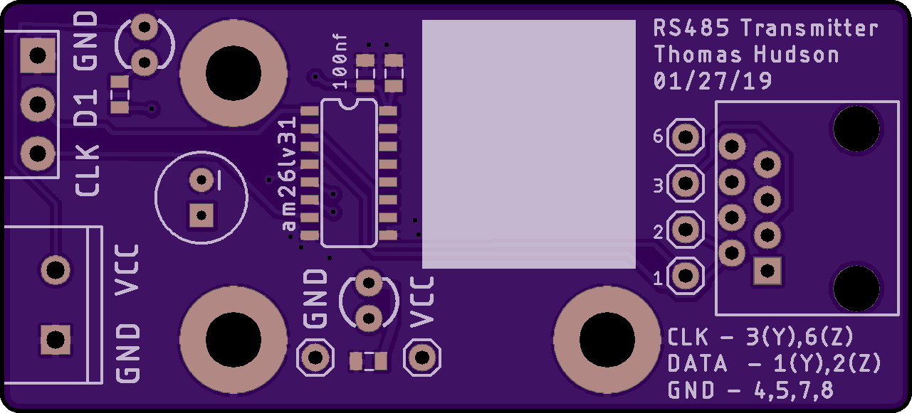
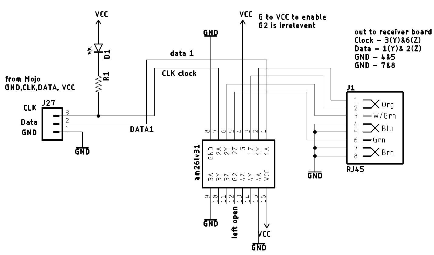
The transmitter board takes two SPI signals (Clock and Data) and passes the signals through an RS485 transmitter chip. The differential signals are routed to an ethernet jack. This board could have been integrated into the Mojo shield to reduce noise but my disigning, programming, prototyping, and installing timelines compressed the schedule and I had to learn as I went. Oshpark files here. See github for source files.
* transmitter chip: Texas Instrument AM27LV31 296-24690-1-ND
* RJ45 ethernet jack: 380-1316-5-ND
*
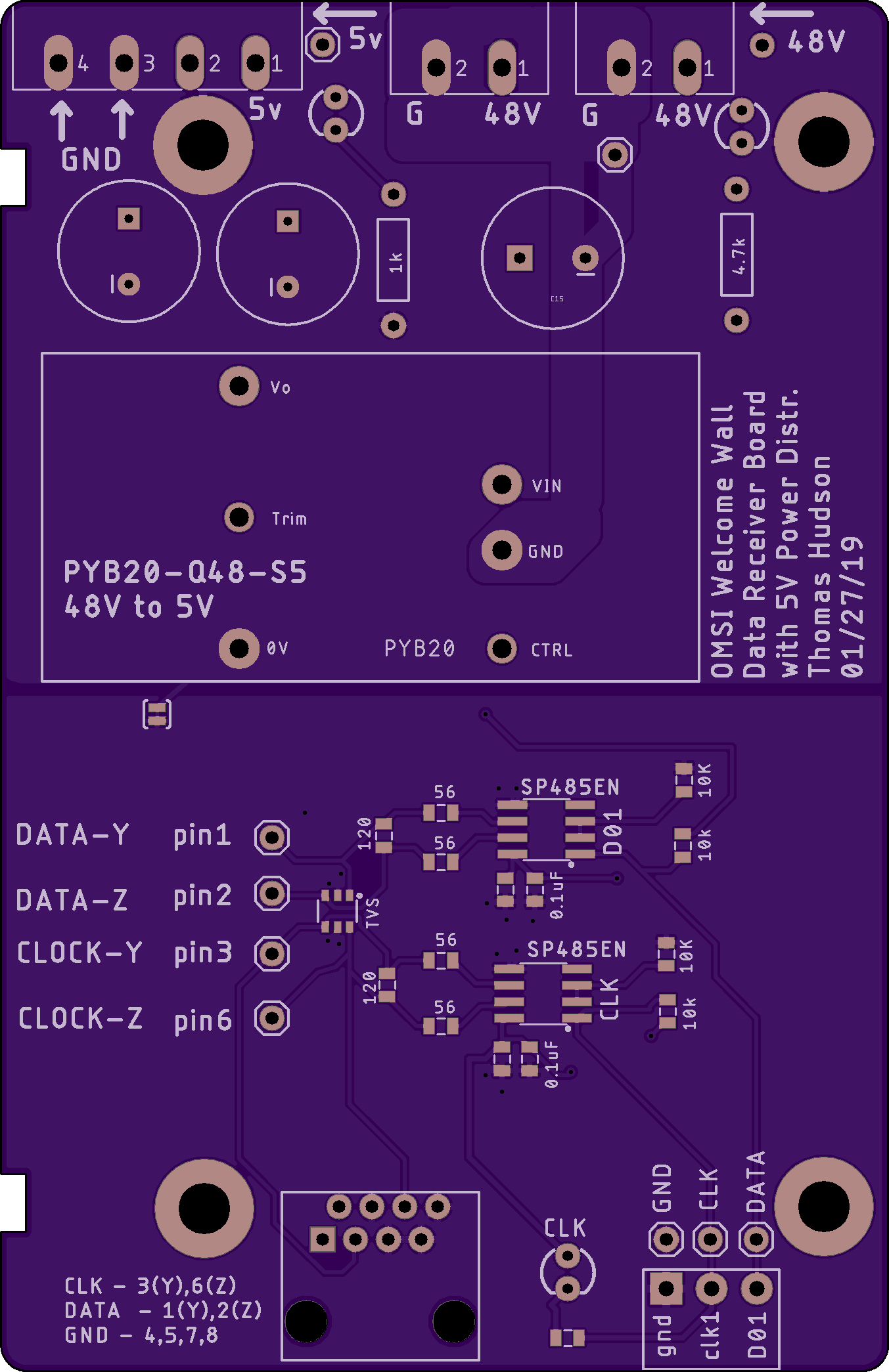
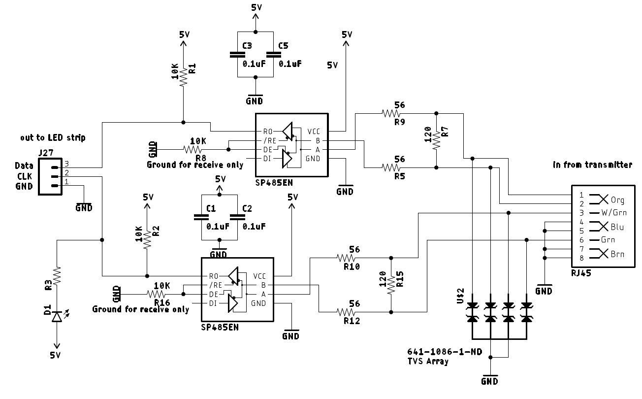
The receiver board receives RS485 signals via a RJ485 ethernet jack. Converts the two differential pairs back into clock and data SPI signals and connects to one LED panel. The board also has a DC-to-DC converter that takes 45V to 5V to supply to the LED panel. I did not put the TVS protection diodes on the boards but added them on just the last few boards I made when troubleshooting noise issues. Also, in addition to the 120ohm termination resistors on the RS485 bus, the original boards have 4.7k pullup and pulldown resistors on the bus. Modern RS485 chips have whats called "failsafe" against idle(no Data) conditions that these resistors are meant to deter.... so I left them out of these last few single signal boards shown here. Oshpark files here. See github for source files.
- Trnsceiver Chip: SP485EN, 1016-1829-1-ND
- RJ45 Ethernet Jack: 380-1316-5-ND
- DC-DC converter - PYB20-Q48-S5
- Mojo Development Board - https://alchitry.com/products/mojo-v3
- HDMI Shield - https://alchitry.com/products/hdmi-shield
- RS485 transmitter chips - https://www.digikey.com/product-detail/en/texas-instruments/AM26LV31EIDR/296-24690-1-ND/2092512
- RS485 transceiver chips - https://www.digikey.com/product-detail/en/maxlinear-inc/SP485EN-L-TR/1016-1829-1-ND/3586546