 Ben Holmes
I've posted this project on reddit asking for a review of the schematic and layout, but the images seem to be dodgy imgur, so I'm posting them here too. Also available on imgur: https://imgur.com/a/UPDZnNs
Schematic
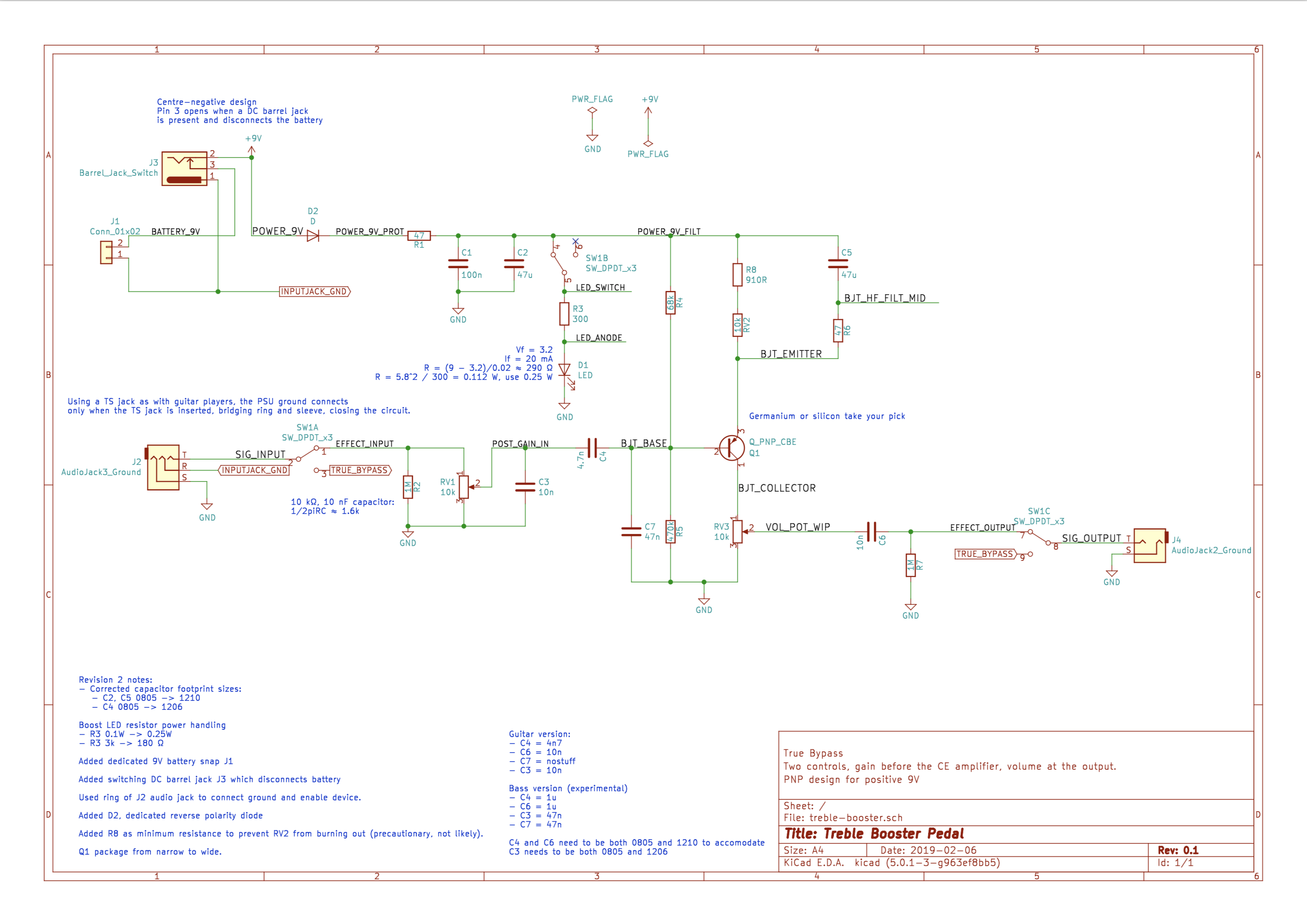
Schematic notes
The circuit is left completely open unless a TS jack is present at J2, which then makes the ground connection between INPUTJACK_GND and actual ground. This is to prevent wasting power.
J3 is a switching barrel jack that disconnects the battery when a 9v jack is present. There's no overvoltage protection for now, but D2 prevents reverse polarity. The voltage drop of D2 (0.7V) is fine because the desired goal is distortion anyway.
The main version of the schematic is for guitars, but I want to make one for a bass playing friend for which I've noted alternate stuffing options. These result in odd footprints where I'm placing both 0805 and 1210 or 1206 to fit bigger capacitors and let more bass through. It's not really a treble boost pedal anymore when I do that! But it's only experimental.
The pedal is true bypass which means there are no components in the signal chain when the effect is disabled. To prevent the switching artefacts from being too bad R2 and R7 pull down the DC blocking caps.
PCB layout, bottom
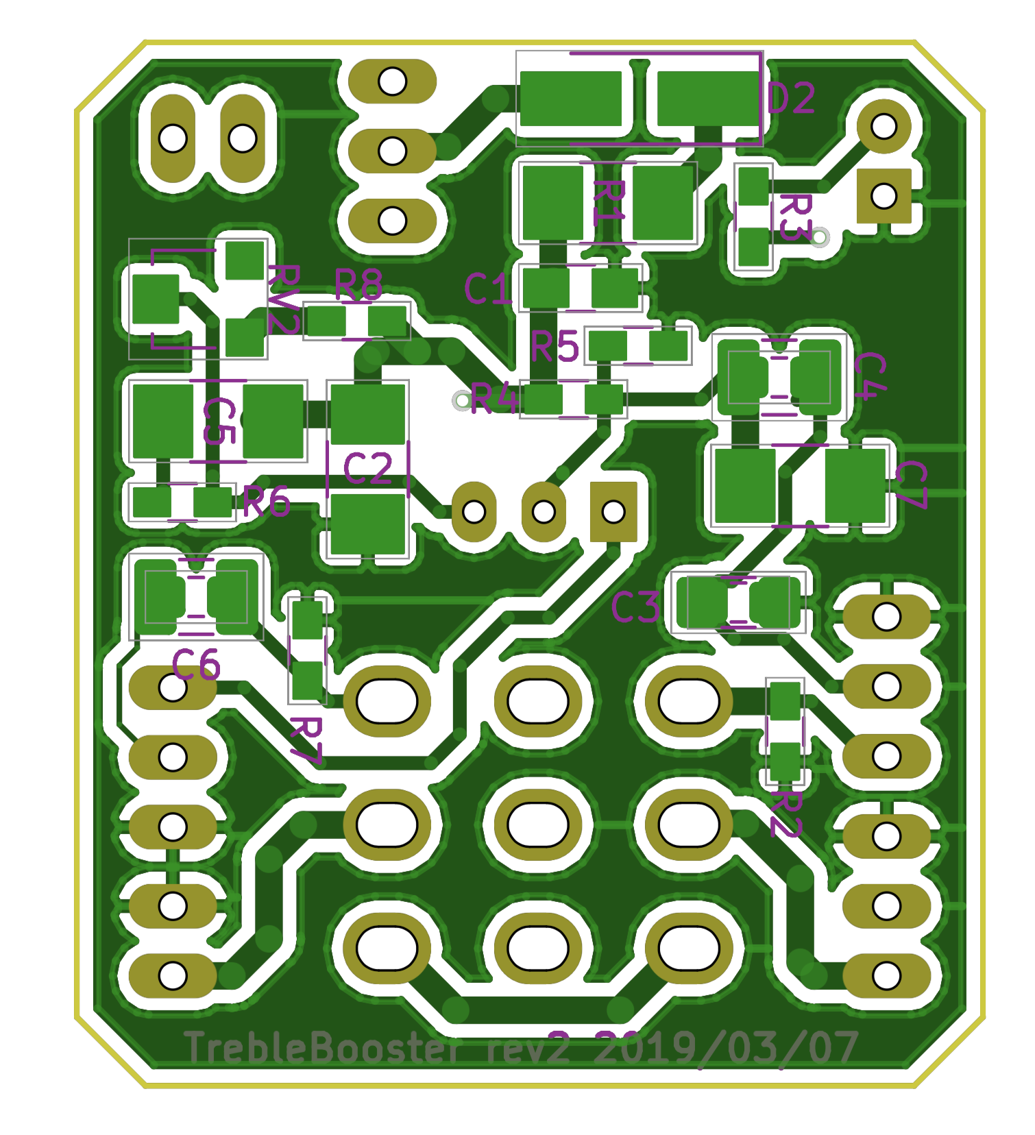
Bottom copper, solder mask, and silkscreen notes
Copper pour is GND.
C3, C6, and C4 all have dual footprints to enable different stuffing options for bass and guitar.
The actual ground return will run out of the ground pad next to the R2 indicator, up to the input jack connector and back to the board.
The only real custom footprint on here is SW1, the large 9 pads in the middle. I designed this from measurements of a 3PDT footswitch that the board will be soldered to directly. This might not be ideal from a vibrations perspective...
All other hardware is offboard and will be mounted in the enclosure itself.
PCB layout, top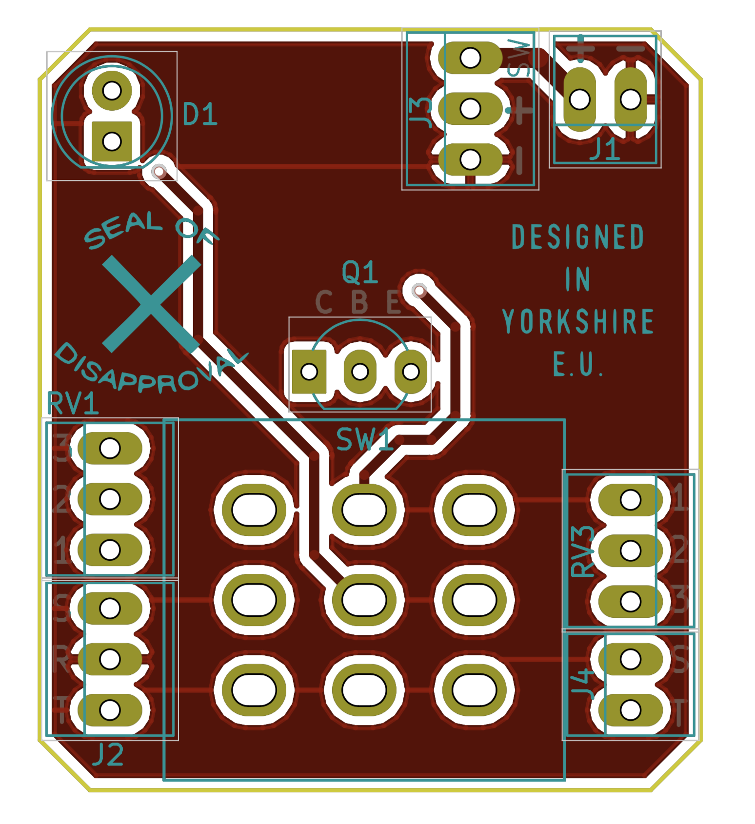
Top copper, solder mask, and silk screen notes
Copper pour is INPUTJACK_GND, trying to make both GND and INPUTJACK_GND super low impedance and with good connection through the offboard jack. Typical edgelord silk screen items to make the PCB seem cool. Ignore political opinions.
BOM
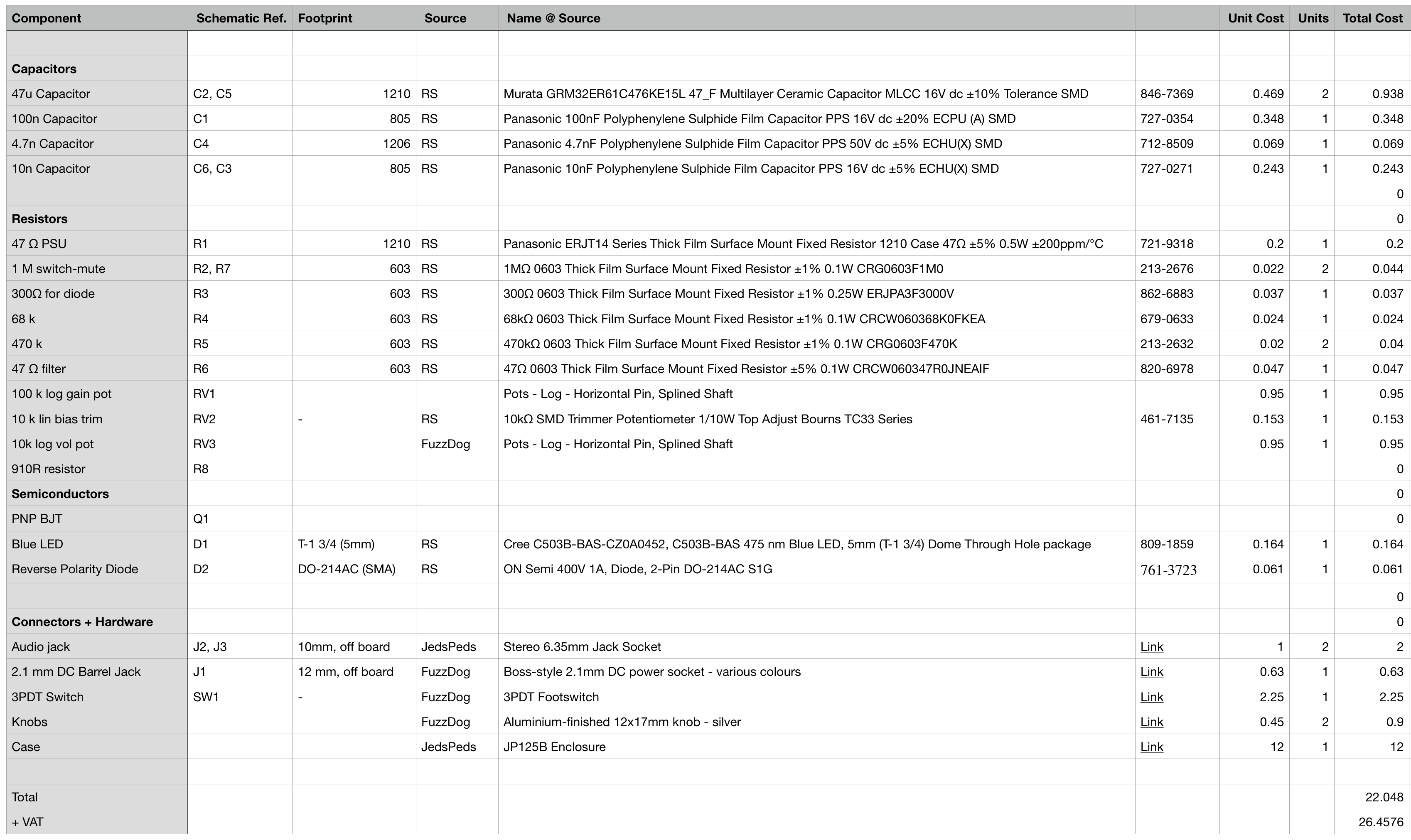
BOM notes
There is a different stuffing for the bass version as noted, but I didn't thing it would be necessary to add here.
Some elements are missing complete information which I will rectify, but again probably not necessary for a review.
Thanks for reading!
Discussions
Become a Hackaday.io Member
Create an account to leave a comment. Already have an account? Log In.