 Plasmode
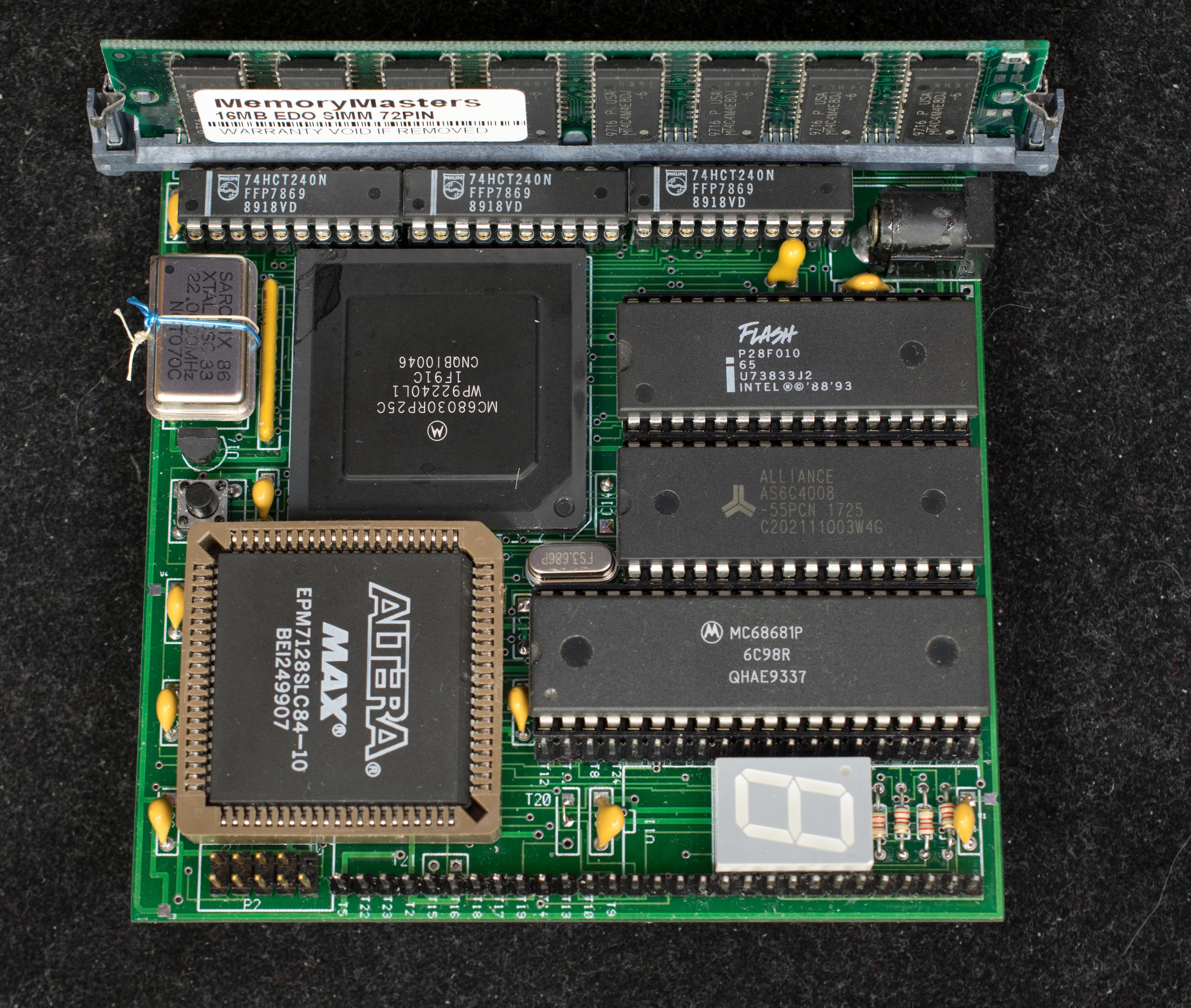
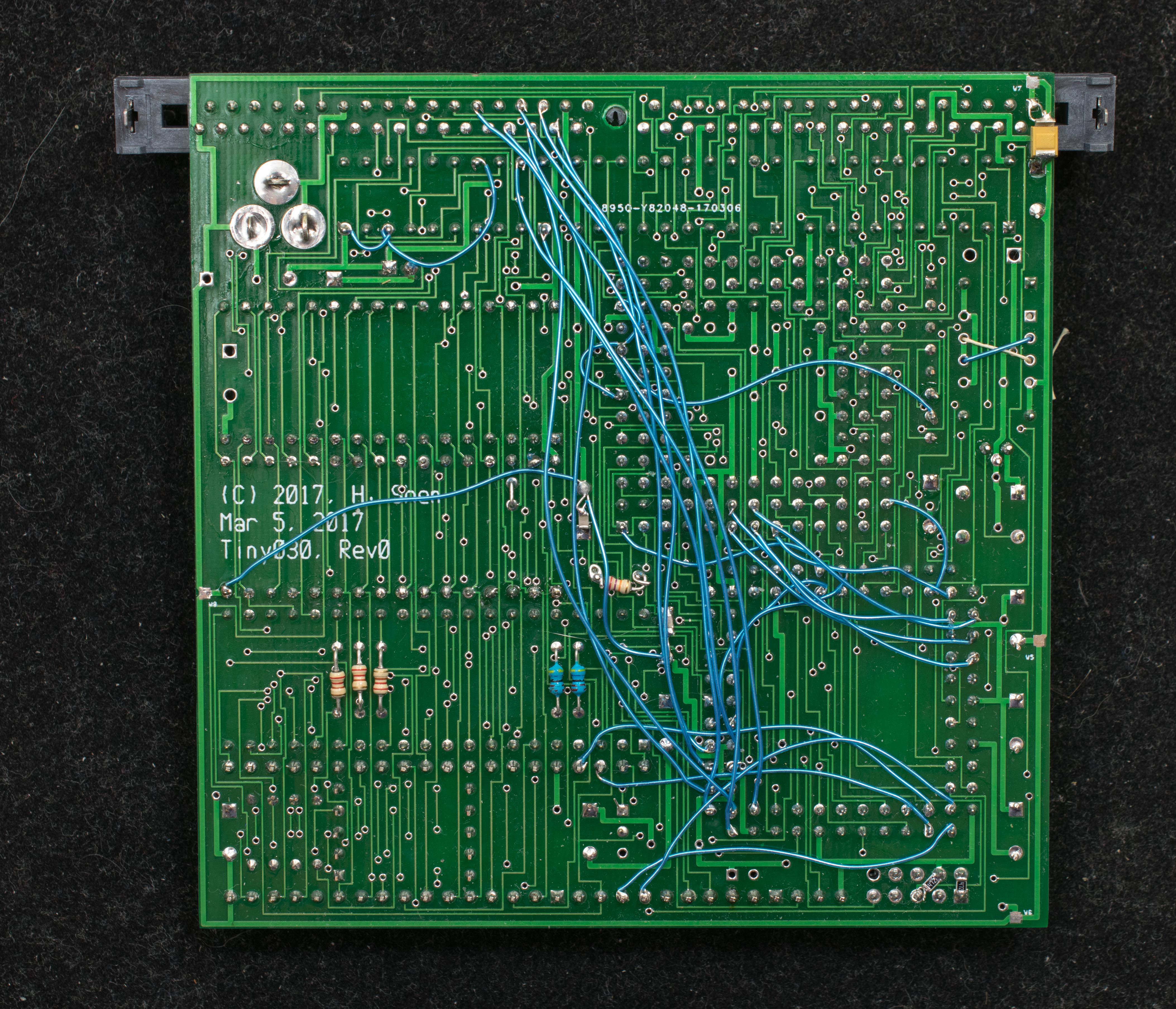
Stage 4 hardware construction is manual intensive. Installing U6-U8 (74HCT240) and socket for 16meg SIMM72 memory are straightforward, but there are many DRAM-related connections that are not hooked up in pc board. Here is a list of connections that need to be manually wired:
| Signal | CPLD pin | 68030 pin |
|---|---|---|
| A21 | 34 | A8 |
| A22 | 35 | B7 |
| A23 | 36 | A7 |
| A24 | 37 | A6 |
| A25 | 39 | B6 |
| Signal | CPLD pin | SIMM72 pin |
|---|---|---|
| nRAS | 76 | 44 |
| nCAS0 | 81 | 40 |
| nCAS1 | 80 | 43 |
| nCAS2 | 79 | 41 |
| nCAS3 | 77 | 42 |
| nSIMMWE | 73 | 47 |
| Signal | CPLD pin | U7 (74HCT240) pin |
|---|---|---|
| nENCASA | 75 | 1 |
| nENRASA | 74 | 19 |
| Signal | U7 (74HCT240) pin | U7 (74HCT240) pin |
|---|---|---|
| floating Input | 8 | Ground (10) |
| floating input | 17 | Ground (10) |
The CPLD equations will need the DRAM controller and refresh logic added. The refresh is CAS-before-RAS driven by a timer and logic that delays the assertion of 68030 DSACKx signals until CAS-before-RAS refresh cycle is completed. This hidden refresh operation occurs once every 128 clock invisible to the 68030. The DRAM controller is a digital delay tap clocked on rising as well as falling edge of clock. Two wait states are needed to access the DRAM. The design can be improved by using 74157 mulitiplexer to reduce the wait state to 1.
The 16-meg DRAM memory map is from 0x1000000-0x1FFFFFF.
Discussions
Become a Hackaday.io Member
Create an account to leave a comment. Already have an account? Log In.