 Marcel van Kervinck
The idea is to transform the RAM socket into an expansion bus in which we plug a small daughterboard. This little board will have a socket to reseat the original RAM, as well as some glue logic for the new I/O capabilities.
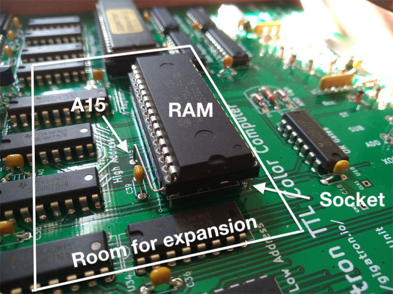
Expanding the RAM
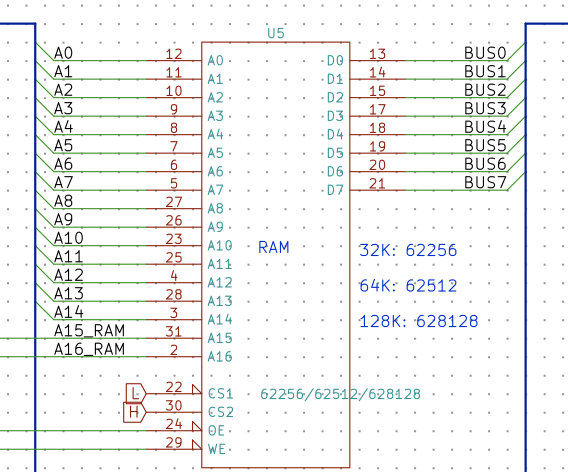
Expanding the memory is an easy by-catch: the original RAM socket is 28-pins for the 32K RAM chip (62256). It has just 15 address lines (A0:14). The sixteenth line (A15) is only available as a breakout on the mainboard. You don't need it for working with 32K, but you need it when you have more memory. If we bring that A15 signal to the daughterboard with an extra wire, we can increase the addressing space. 32-pins memory chips exist in 64K and 128K sizes (62512 and 628128). Their pin layout is compatible: you can put the smaller chip in the larger socket, and it will work!
(Actually, if you just want 64K, you don't even need a daughterboard, as shown on the photo above.)
Access to output
It's a lot less obvious how to expand the I/O: there simply aren't enough user controllable signals going to the RAM socket. Next to the address and data bus, there are only a READ signal (/OE, for Output Enable) and a WRITE signal (/WE, for Write Enable). RAM doesn't need more... One idea is to map the I/O actions into the address space. But this runs into practical issues we won't delve into here.
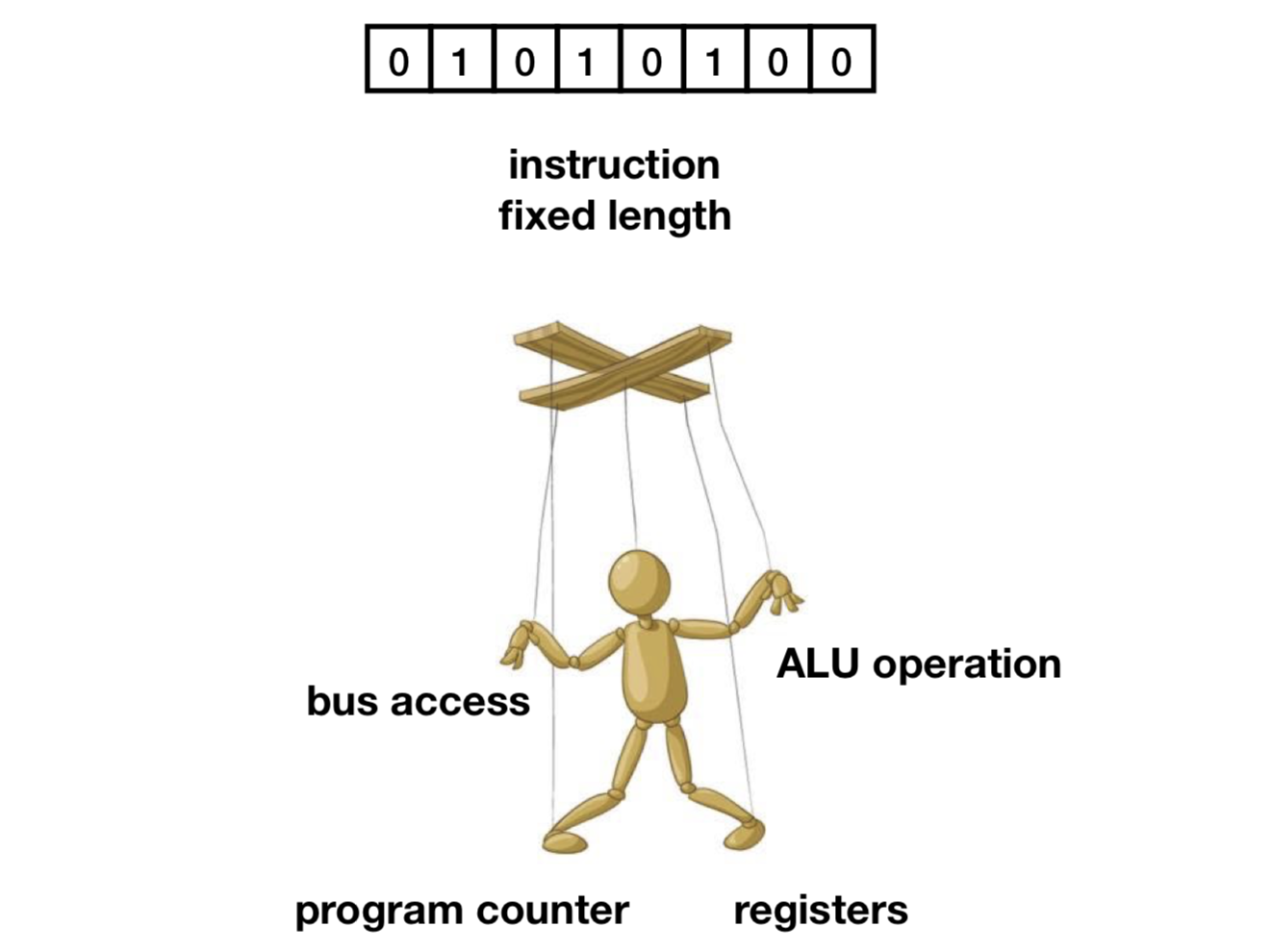
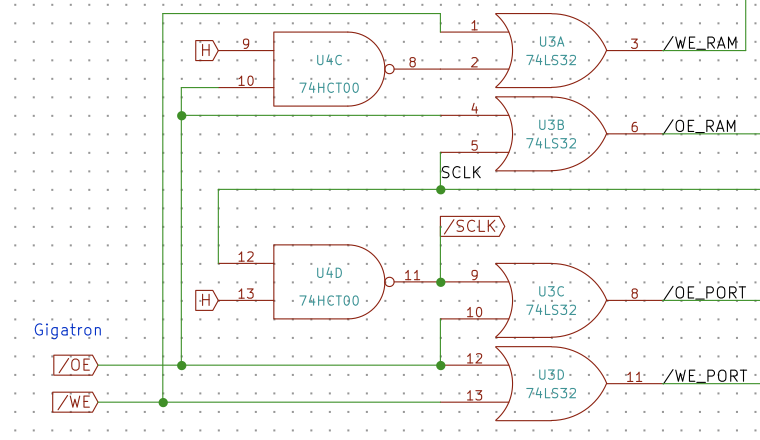
The solution is to abuse the Gigatron's orthogonal instruction set. In the Gigatron, writing is controlled by the upper 3 bits in the opcode. Those bits select the operation. Reading is controlled by the lower 2 bits that determine who accesses the bus.
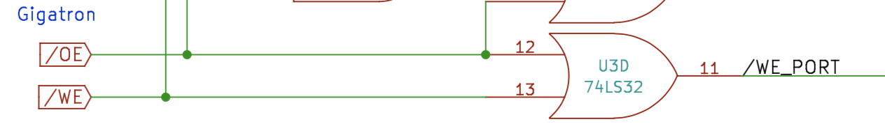
The magic trick is that we can activate a simultaneous READ+WRITE to give access to our new I/O capabilities... No smoke will escape, but normally this combination results in writing undefined data into the RAM. With a little bit of glue logic, we will repurpose this combination to give access to the I/O port:
/WE_PORT = /OE | /WE
We just hacked and extended the native instruction set with a single OR gate! Problem solved. Well, except that the data bus is not accessible when /OE is low, so where does our data go? That will have go on the address bus when we invoke this new mode.
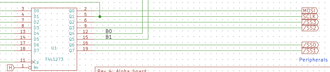
The I/O logic will have one 8-bit register (74x273) for the output lines. We assign each bit a meaning: MOSI, SCLK, /SS0, /SS1, /SS2, /SS3. These signals branch out to four SPI ports (Serial Peripheral Interface).
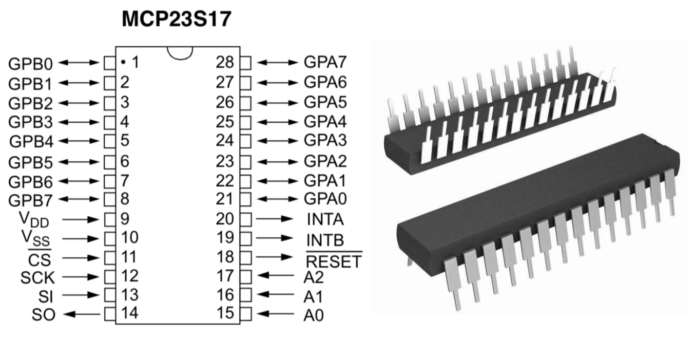
With SPI you can interface with MicroSD cards, sensors and IoT gadgets. There's also the popular MCP23S17 chip that turns a SPI channel into 16 GPIO pins. Imagine the possibilities: a RAID with SD cards? 64 GPIO pins?
Access to input
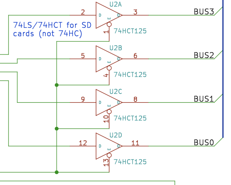
The returning four SPI data lines are fed into a 4-bit buffer chip (74x125) which connects back to the Gigatron data bus. This chip will be allowed to write onto the bus during an I/O action (meaning: when SCLK is HIGH). From a machine code point of view, this looks like a well-timed memory read.
Memory banking
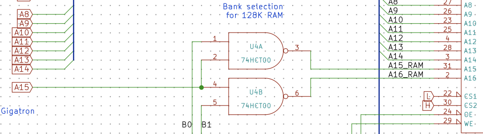
The two remaining flip-flops can be used for banking the memory above 32K. We will fixate the lower 32K of RAM, and allow any chunk of 32K to be mapped into the higher 32K address space. We can support 128K chips this way and not waste a single byte.
Wrapping up
For the glue logic we need an 74x32 (Quad OR) and 74x00 (Quad NAND). And that's all there's to it. Just four TTL chips in total: 74x00, 74x32, 74x125 and 74x273. All the rest is software.
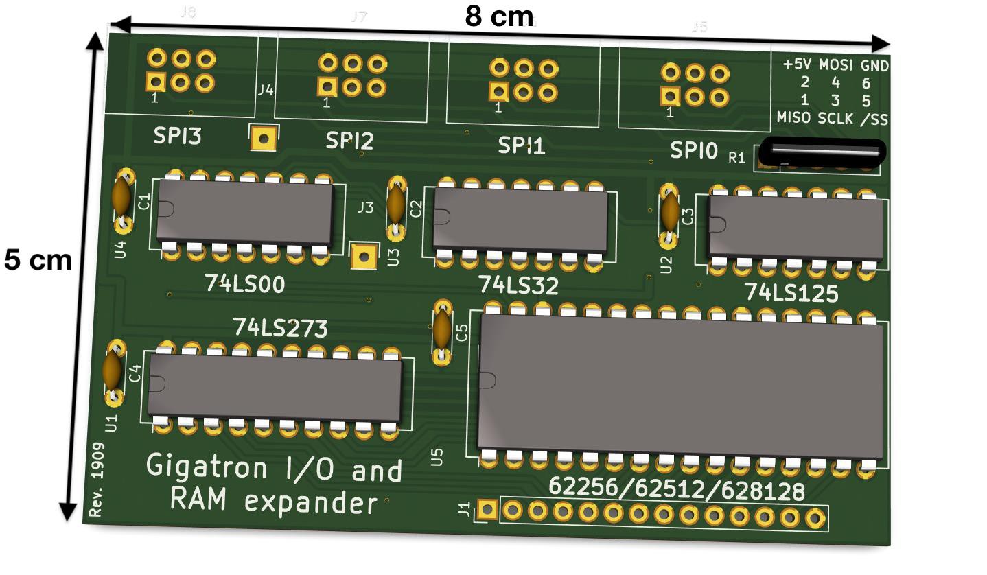
Prototype
The next step is to build it. Here's an 3D rendering of what the board would look like:
Credits
This concept was developed on the Gigatron forum. Special thanks must to [jwolfram], [monsonite] and [nutson] for their invaluable contributions.