 Alastair Hewitt
The remaining instability in the Rev. 1 board is down to power issues. The power distribution was deliberately underspecified to highlight problem areas and test different designs. There are two main areas of concern: inductance and current consumption.
Inductance is the biggest enemy for maintaining a clean power supply. The decoupling capacitors help, but adding multiple return paths to ground seems to be the most reliable strategy. The inductance of each path is placed in parallel, so two paths will halve the inductance of the single path.

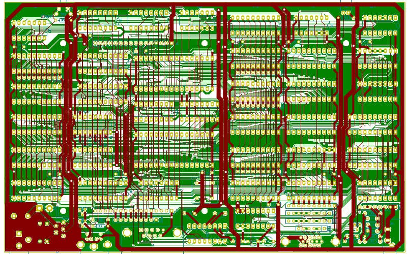
Inspiration was taken from 70's video game boards (an example shown above). These were designed before the introduction of microprocessors and typically required well over a hundred (non-LS) TTL chips. These are arranged in columns of several chips with one or more decoupling capacitors per column and a dual return power path. This is the approach taken for the power distribution on the Rev. 2 board.
The other issue is the relatively large current consumption at 1.5A. This is just for the core system and doesn't include additional power to things like a WiFi dongle (2W) or expansion board (300-500mA). This pushes the maximum current consumption closer to 2.5A and poses some major challenges in maintaining the supply voltage between 4.75v and 5.25v
The initial plan was to use a 5v power adapter and there are plenty of inexpensive options to meet the current requirements. The problem with these is the resistance between the power supply and the power distribution on the board. The leads from the supply and resistance of the barrel jack connector comes in over 300 milli-ohms. This would drop the voltage by 0.75v at 2.5A, resulting in only 4.25v getting to the board power rails. Some 5v supplies output 5.25v to compensate, but this still means the supply would only reach 4.5v on the board.
One idea was to start with a higher voltage like 6v and add some additional resistance to drop the voltage down to 5v. The 6v supplies also tend to compensate and typically output 6.3v, so adding a 0.22 ohm power resistor to the supply line would drop the voltage to 5v (assuming a total resistance of 520 milli-ohms). This assumes a current consumption of 2.5A, but the base system consumption of 1.5A would result in a supply of over 5.5v if the additional components were not used with this approach.
What's really needed is a regulator on the board. One option is a linear regulator to take a 9v or 7.5v supply and drop it down to 5v. Again the current consumption poses a problem here resulting in up to 2.5W of heat dissipation for each volt dropped. Low-dropout regulators are available, but these would still result in over 4W of dissipation and require a large heatsink. The other option is a buck converter and this is the current plan for the Rev. 2 board.
There are inexpensive SMD modules that can fit in the available space, but these don't have the best thermal design or reliability. The components are available in through-hole however and the buck converter can be added directly to the board. A small heatsink is required and this can be wrapped around one of the mounting holes to maximize the available space as shown below.
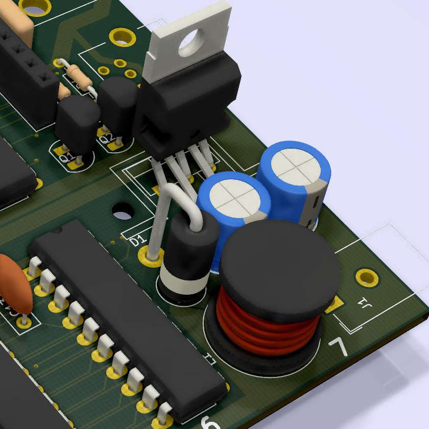
This design can use a much higher voltage and avoid the large input current and voltage drop getting the supply to the board. The current power supply design would only need 600mA using a 24v supply. This includes 2W of direct power to the Wifi dongle and provide up to 2A at 5v via the buck converter for the main system and optional expansion board (assuming 80% efficiency). Heat dissipation is also a more manageable 2W with this design.
Discussions
Become a Hackaday.io Member
Create an account to leave a comment. Already have an account? Log In.