Today I finished the schematic of the main computer board (the first version, I guess...). You can find it in the file section, and the most important parts will be discussed here.
SYSTEM INPUTS AND OUTPUTS

The 24 system outputs can be directly controlled by microcode instructions. [updated 20190723] They are used for:
- video control
- SPI bus
- selecting shift modes for the B register
- enabling upper- or lower byte of video- or main memory
- selecting a system input, together with OP6 (instruction bit).
The system inputs can select from 8 input signals. Normally, IN_SEL0 and IN_SEL1 are zero, and the instruction bit OP6 selects between NON-ZERO condition or D0. So, instructions that check for zero must have bit 6 one. Instructions that check the lowest address bit A0, for enabling high or low byte, must have bit 6 zero.
For selecting keyboard or mouse signals, IN_SEL0 and IN_SEL1 must be written first. It is expected that polling these signals in the video-line interrupt will be just (barely) fast enough to read them.
VIDEO ADDRESS GENERATION
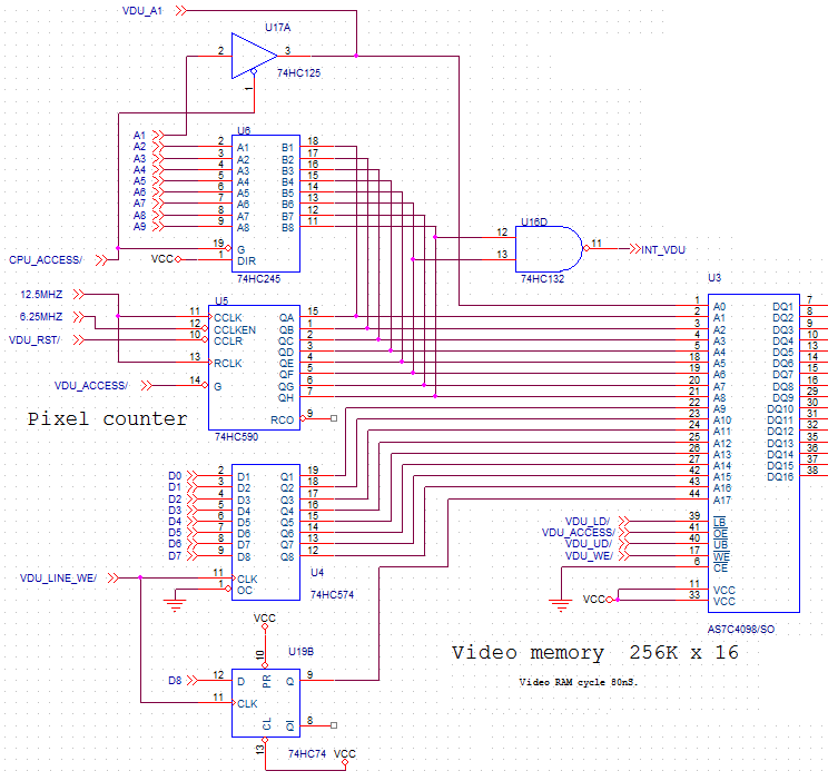
Next comes the video address generation. There are two situations:
- The video system is in control and reads the pixel data from memory. CPU_ACCESS/ is not active, VDU_ACCESS/ is active (low). Address bits A1 - A8 come from the pixel counter (changing every 160nS). Address bit A0 comes from the VDU_A1 signal from the timing generator (changing every 80nS). Address bits A9-A17 come from the 9-bit register formed by U4 and U19B. The NAND gate will generate an interrupt for the CPU when the count is 160 (128 + 32). The interrupt will end when the count is 192 (128+64). The end of the interrupt is important, because that is used by the CPU to exactly synchronize to the video signal, in order to generate exact horizontal sync signals and resetting the pixel counter on time.
- The CPU has control and can write pixel data to the video memory. CPU_ACCESS/ is active, VDU_ACCESS/ is not active. The output of the pixel generator is now disabled, and the address bits A0-A8 are now delivered by the buffers U6 and U17A. Note that the pixel counter keeps running. The video memory output is disabled.
VIDEO DATA HANDLING

When the VDU is in control (pixels read from memory), two pixels are read every 80nS and delivered in the registers U9 and U10. Seven outputs of the registers are connected to the resistor-based D/A converters that generate the voltages for the RGB signals. The timing section will determine if U9 or U10 delivers its data to the D/A converters.
- In HIRES mode, both pixels will be sequenced, so each pixel will be visible for 40 nS.
- In DUAL LAYER mode, bit 7 of pixel two determines which pixel will be displayed during this 80 nS cycle.
When the CPU is in control, it can write its data through the buffers U7 and U8 to the memory. The control section will in this case not enable the PIXEL_CLK, so the video output keeps displaying the same pixel (black).
TIMING SECTION
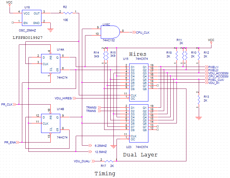
The timing source is at the upper right. This should be a 25.175MHz oscillator, but that is only available in 3V3 version, so I took a 25MHz 5V oscillator and hope the monitor will handle it.
The two flipflops below the oscillator divide the clock down to 12.5 and 6.25 MHz. The NAND gate generates the 6.25 MHz CPU clock. It is only active (low) 1/4 of the time, this is needed because the CPU contains some latches instead of flipflops, and we must be sure that the correct latch is selected before the clock goes low. This asymmetric clock gives more time to select the correct latch.
The two 8-bit registers control the video section. The CPU can write to the video memory when both are disabled. Only one should be enabled at a time.
When the upper register is enabled, control signals for HIRES mode are generated.
When the lower register is enabled, control signals for DUAL LAYER are generated.
Next thing to do, is design a PCB for the main board.
Discussions
Become a Hackaday.io Member
Create an account to leave a comment. Already have an account? Log In.