Overview:
For a span of 3 months, my project/task is to create/add more features to a simple LED driver. At first, you might think that a three-month timeline seems too long for this project, but having the available time only on weekends and weekday evenings could really drag the project out.
Initially, this project was meant to be used in mirror lighting applications... you know, those lights installed around the edge of a girl's mirror, because apparently, their room lights aren't enough to illuminate their painted faces while doing their "thing", or their "artwork". However, I usually find these things in the women's parlor and it uses 110V/220V lamps with some having just the basic ON/OFF function. So I got an idea...
**************************************************************************************************************************
PART 1
Why this project?
The main reason I'm doing this project is because someone made me do it. I didn't like the idea of using AC lamps so I thought I might use 12V led strips instead. They're smaller, can easily be installed since you can stick them directly on the mirror, they are robust and can be upgraded easily by extending or adding more strips. Additionally, I already have a 12V SMPS power supply intended to drive these things, which are also readily available in almost any electronics shop. However, a simple LED driving circuit feels boring to me, so I thought about adding features that would make the device more versatile.
Lately I've heard about projects related to smart farming and in a distant future, I was thinking of making a somewhat related project that focuses on artificial lighting.. but I didn't know that that would be this project. I thought that I can just turn this simple LED driver project into something that is applicable also to artificial lighting.
The LED mirror lights and the artificial lights that also uses LED in smart farming applications basically do the same thing. They turn ON/OFF the LED with brightness adjustment. The difference lies on the feedback wherein artificial lighting takes into account the ambient light and also has a target value for illuminance. On the other hand, the brightness control of the LED mirror lights simply depend on manual adjustments from the user.
Given this intended dual application of the device, I'll opt to use some modules to enhance the feature set that caters to both scenarios and even wider range of scenarios. This will be discussed in the succeeding paragraphs.
Intended Application:
Initial intended application:
- Home lighting (mirror lights)
- Temperature, humidity, ambient light, smoke/gas monitoring with data logging
- Mobile/mini smart farming stations
Intended Features:
Since this is part of the initial planning, some of these features might not appear in the actual implementation. Each individual feature will be explored as I continue working on this project but for now, here's what I would want to have in this device:
- LED Drive, 12V, up to 10A total in 2-channels with current monitoring
- Temperature Sensing
- Humidity Sensing
- Gas detection
- LCD status display
- (SMS capability)* --> WiFi/Internet access capability
- Data logging
- Ambient light sensing
- Overcurrent/Overvoltage supply protection
***UPDATE*** - Changed the #6 feature from SMS to WiFi due to problems I encountered in my SIM800EVB board module. I searched a few similar issues in the internet and it seems like this board is actually problematic.
Initial Specifications:
For the initial technical specifications, I'll just list the things that appears on my mind as of this moment:
- Supply input: 12V, 12A
- Max LED load current: 10A
- Adjustable data logging interval: 1sec - 28800sec (8hrs)
- Adjustable LED brightness: 0-100% PWM duty cycle
Other specifications will depend on the individual modules to be used.
System Block Diagram:
The following diagrams are rough sketches of the initial system. Please don't judge my drawing skills :)
A. Power Section
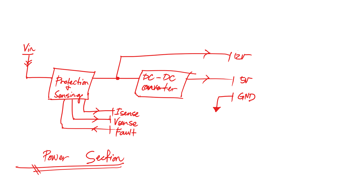
B. LED Driver
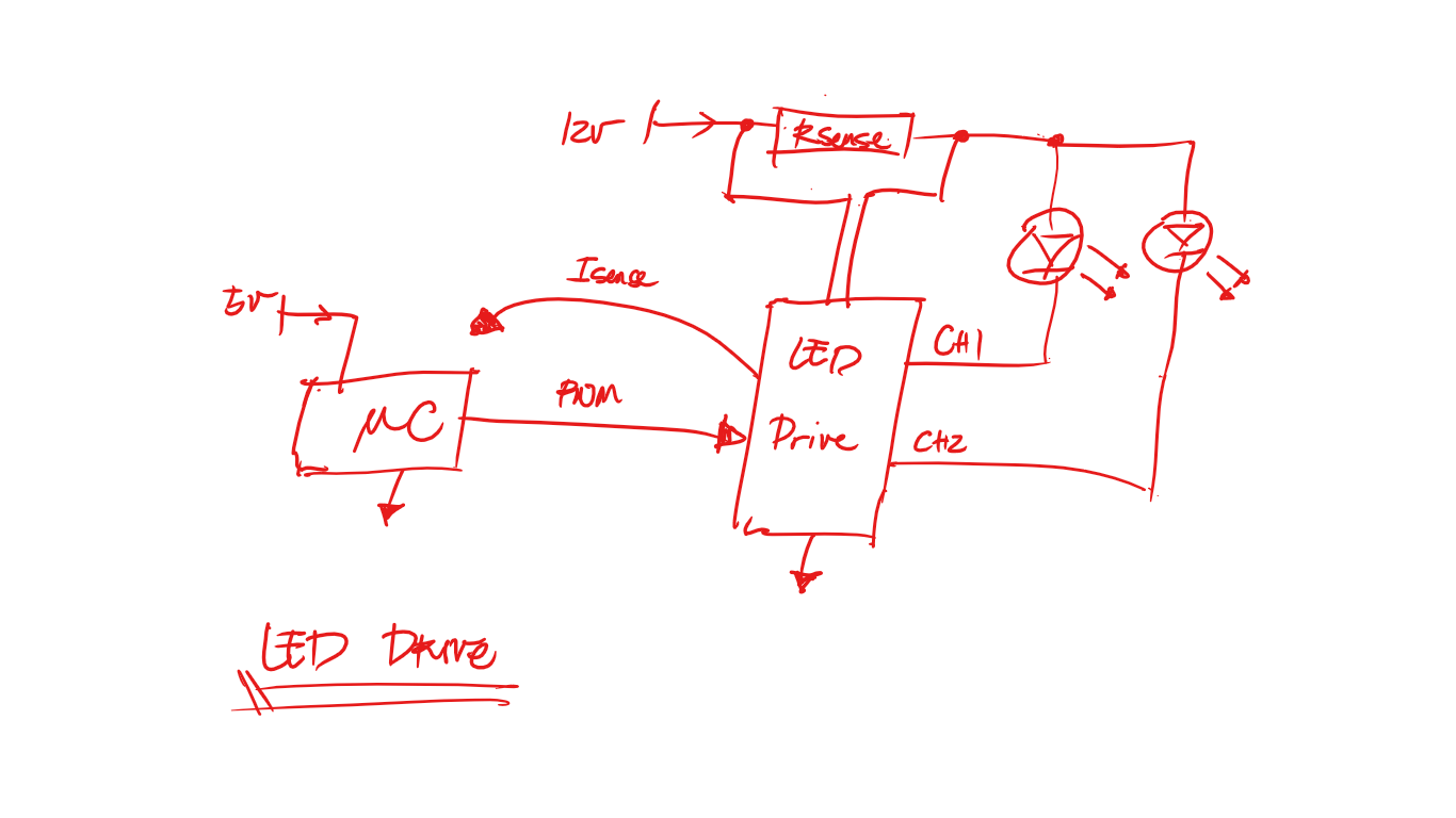
This setup enables two ways of controlling the LED. Either I opt for current control, or just the more basic voltage PWM. The in-depth discussion on this will appear in a future part of this series.
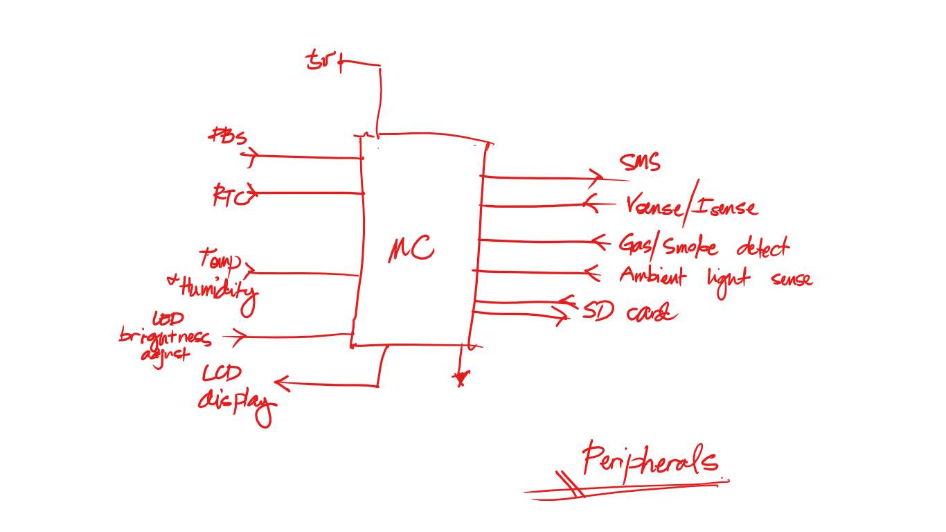
C. Peripherals
Initial planned out implementation:
Looking into what might be the actual hardware implementation, I'm listing all my ideas below:
- PCB fabricated 2 layer board
- SMD package for passive components
- Board size is module dependent
- Use an I2C interface board for the LCD module (16x02)
- Peripheral section will use readily available modules and the board will allot space for each individual modules to be soldered
- Power Section and LED drive section will be custom designed and will be embedded into the board
***END OF PART 1
**************************************************************************************************************************
PART 2
Power Section - Features and Specifications
The power section will have a few protection features that would minimize the occurrence of common fault conditions namely:
- Reverse polarity or improper input supply connection
- Over voltage (OVP), up to 30V
- Over current (OCP)
NOTE: If you don't have a background knowledge on circuit protection, I also have a 2 part video tutorial on this that talks about basic circuit protection schemes which you can find in the following links:
Tutorial Part 1:
Tutorial Part 2:
Now back to my project documentation:
The device will be rated at 12Vdc input so it is assumed that the user would supply it with the appropriate voltage. However, there is a need to consider very rare scenarios where a user might accidentally connect a 24V car battery instead, or use a laptop charger. In this case, it is worth putting an OVP feature in the device to ensure safety. As will be shown later on, this OVP feature can only handle up to 2.5x the rated voltage, and beyond that, the protection circuit will be damaged. On the other hand, the OCP feature is in charge of shutting down the device whenever a huge current flows into the power rail, and unlike the fuse which needs constant replacement, the device make use of a sense resistor to detect the over current scenario.
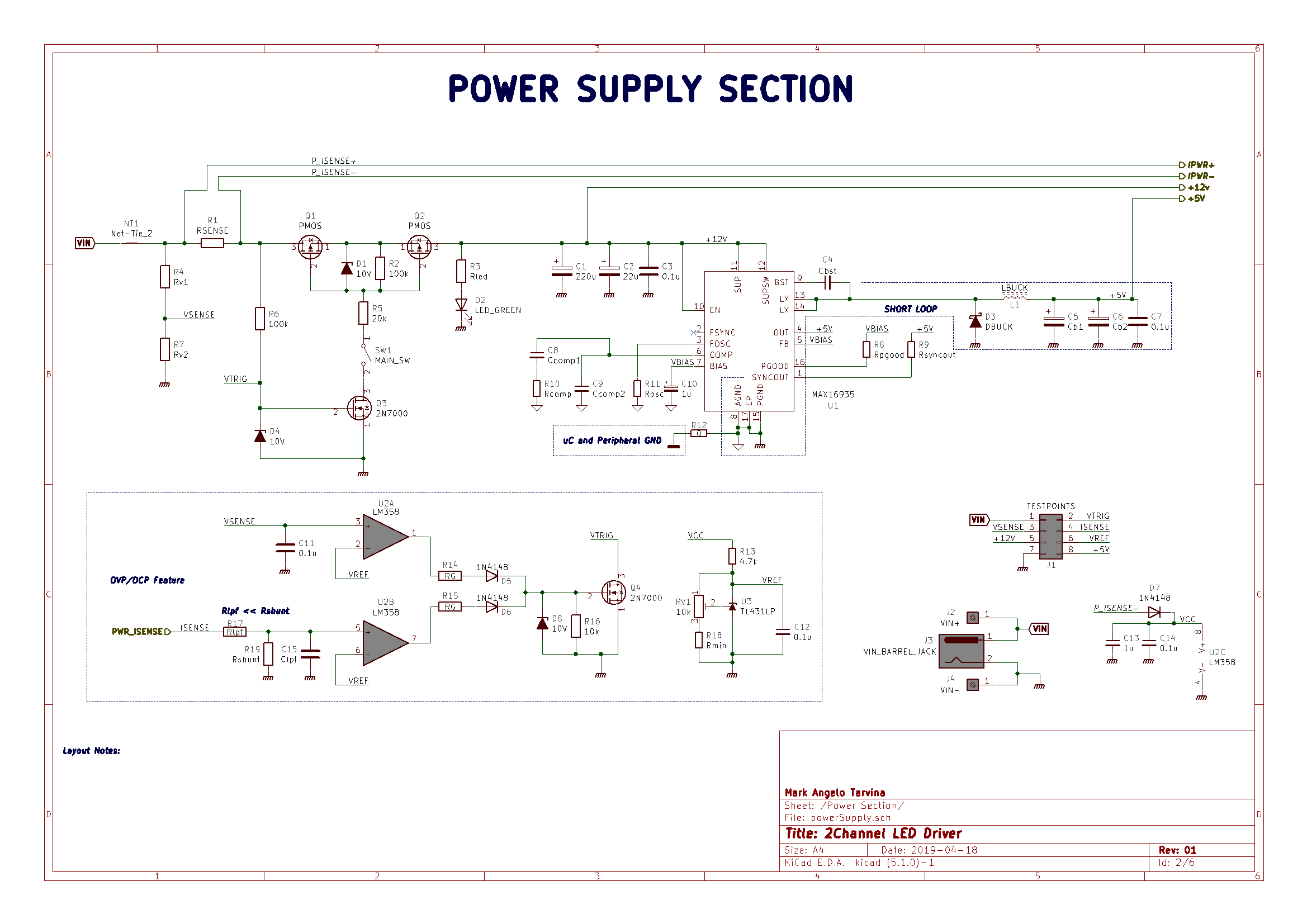
Power Section - Full Schematic
The whole power section contains three main parts namely: the main power switch, the OVP/OCP circuitry, and the buck converter for the 5V rail. I will dedicate the 3rd part of this documentation to the buck converter, and will focus on the other two main parts at this point.
Power Section - Main Power Switch
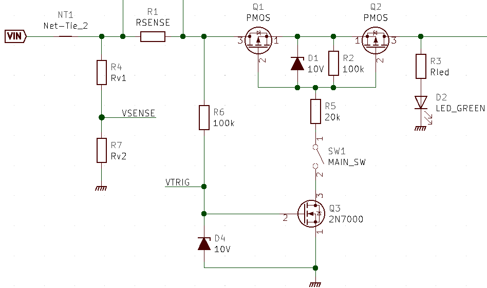
The main power switch is composed of two back to back P-channel MOSFETs, Q1 and Q2, having the same turn on condition set by D1, R2, R5, SW1, and Q3. This configuration allows me to use a low power switch that is more readily available in a smaller form factor, rather than buying a larger switch with high current rating, which is more expensive. This also allows the system to override SW1 and shutdown the system automatically during FAULT condition.
The zener diode D4 prevents excessive Gate voltage that may trigger Q3. Resistors R4 and R7 are used as a voltage divider to sense the input voltage level. This signal will be fed into the OVP circuitry to determine if an over voltage condition occurs. The RSENSE resistor will be responsible for sensing the current consumed by the whole circuit by converting this current into a voltage signal fed into the OCP circuitry.
At startup, the main power switch will operate as follows (initially SW1 is OPEN) :
- Vin is connected into the circuit
- The sense voltage will be present immediately after connecting Vin. At this point, the OVP circuitry is already active, while OCP is still inactive.
- Vin turns ON Q3 through R6, provided that there is no over voltage condition, which sets the control circuitry connected to net VTRIG to be of high impedance.
- Current can already flow through Q1 due to its internal body diode, but could not pass through Q2.
- When SW1 is CLOSED, both Q1 and Q2 turns ON, delivering power to the rest of the circuit and powering up the 5V rail, which now enables OCP.
- The OVP and OCP circuitry constantly monitors the input voltage and input current.
- Whenever a FAULT condition occurs, either OVP or OCP, then VTRIG is shorted to GND which in turn, turns OFF Q3, and as a result: turns OFF Q1 and Q2.
Power Section - OVP/OCP Circuitry
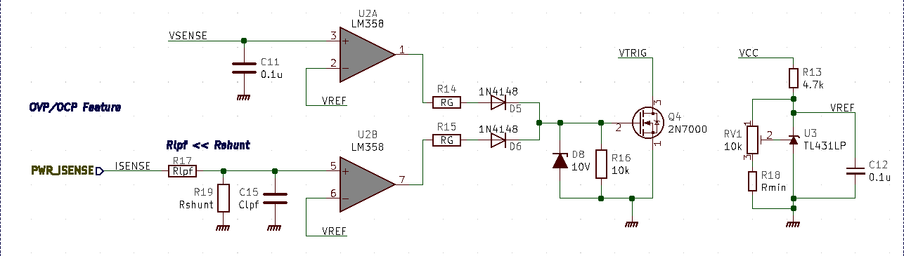
The OVP/OCP circuitry is made up of two comparators each responsible for comparing the voltage and current signal to a reference voltage set by U3. The outputs of the two comparators are then used as inputs to the OR gate composed of D5 and D6 which in turn triggers Q4, the transistor responsible for setting the state of the node: VTRIG.
NOTE: The operating voltage range of the LM358 is only up to 32V in a single supply configuration. This limits the maximum allowable over voltage detection range in which the op-amp will still function properly. Putting a much higher voltage at the input will totally damage the protection circuit. Still, since the device will be rated at 12V, any over voltage fault condition will be assumed to be within the range of 15V to 30V given that common DC power supply nowadays output voltages in this level, especially in the automotive systems where 12V and 24V rails are commonly employed.
Power Section - OVP Simulation using LTSpice
To test if the OVP circuitry will work as expected, I created a similar circuit in LTSpice to simulate an over voltage scenario. The schematic and the output waveforms are shown below:

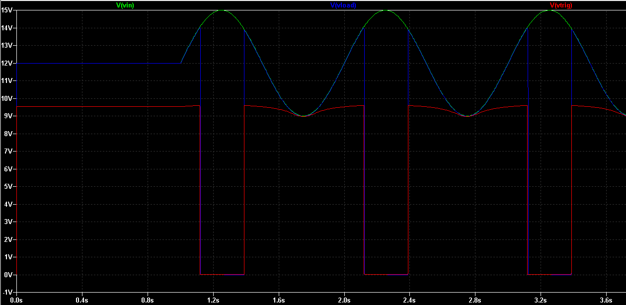
The OVP trigger voltage is set to 14V and the input voltage used is a 3V peak sine wave riding in a 12Vdc supply. When the input voltage reaches the 14V level, VTRIG is shorted to GND, and the input is then disconnected to the load.
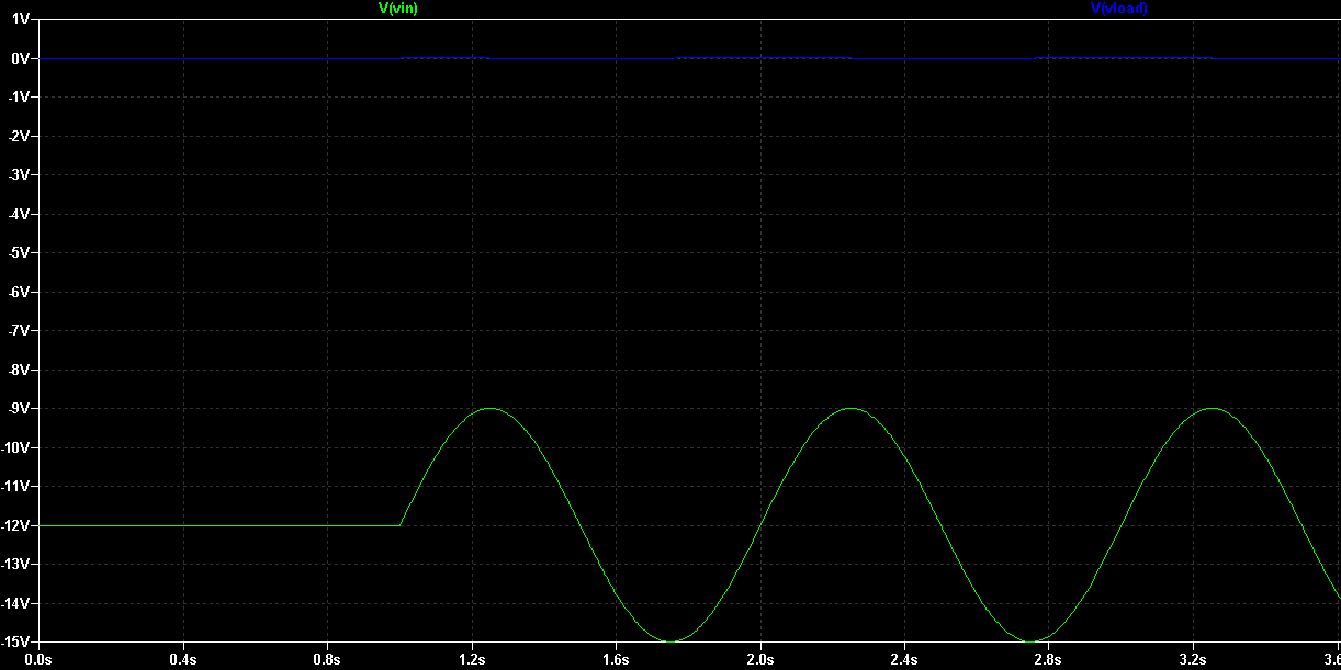
When the input supply voltage is connected in reverse, then the output stays at 0V, proving that the reverse protection works as shown in the waveform below:
P.S. I'm still yet to decide on the trigger voltage for the OVP as well as the trigger current for the OCP. I'll update this documentation once I've finalized the design for the system as a whole.
***END OF PART 2
**************************************************************************************************************************
PART 3
Buck Converter - Features and Specifications
The buck converter of the power section only has 3 main specifications:
- Vin: 12V
- Vout: 5V
- Iout, continuous (max): 2A
For the sake of rapid prototyping, and since this is not the main focus of the project; I prefer to use a dc-dc controller IC with the lowest external parts count as much as possible to simplify the layout and reduce components listed in the BOM. Upon searching in my component inventory, I found something that perfectly fits this project's specification.
Buck Converter - Schematic

For this project, I'll use the MAX16935: 36V, 3.5A, 2.2MHz Step-Down Converter. It's maximum 3.5A specification is more than enough for my 2A requirement. It can accept input voltages up to 36V, and has a simplified circuit configuration for setups requiring a 5V rail. The high side switch or power FET is already integrated inside the IC, and the system can operate up to 2.2MHz of switching frequency, thus decreasing the size requirement for the inductor.
Normally, one output capacitor is enough in a basic buck converter setup. In this case, its much better the split the output capacitor into 2 parallel capacitors, Cb1 and Cb2, with added 0.1uF bypass to lessen both the overall series resistance of the capacitors and the output ripple. I'm not really concerned about the efficiency requirements of the converter at this point but the datasheet says it only consumes 28uA quiescent current at no load, so thats just a plus I guess.
Buck Converter - Components and Design Resources
In the above circuit, DBUCK is rated at 3A, Cb1 = Cb2 = 22uF, Rosc = 12kOhm and Cbst = 0.1uF for a 2.2MHz operation, and the passive components at the compensation stage are yet to be decided. The circuit is based on the typical application circuit found in the datasheet as shown below:
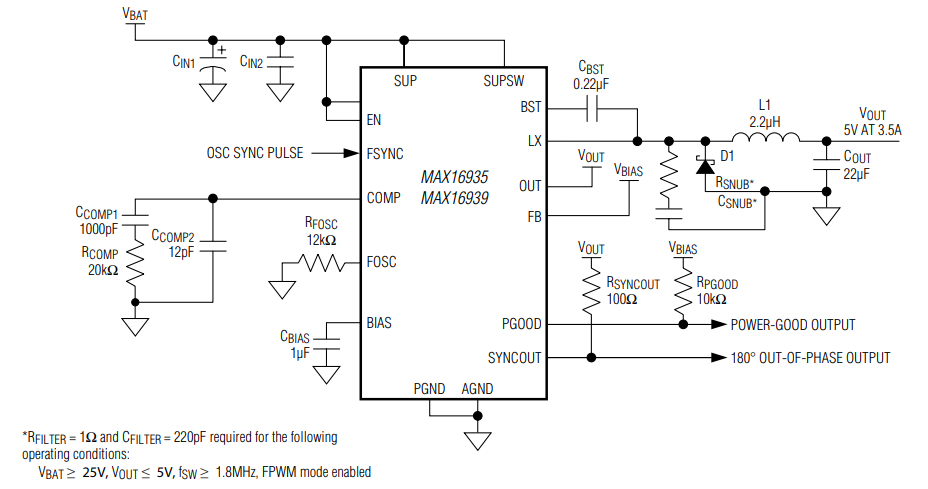
For more information, here's the datasheet link: https://datasheets.maximintegrated.com/en/ds/MAX16935-MAX16939.pdf
In my case, I also tried to check the schematic of the EVKIT that uses the same device and derived my implementation from there. Aside from the schematic, the EVKIT file contains information on recommended board layout as well. The EVKIT schematic is shown below:
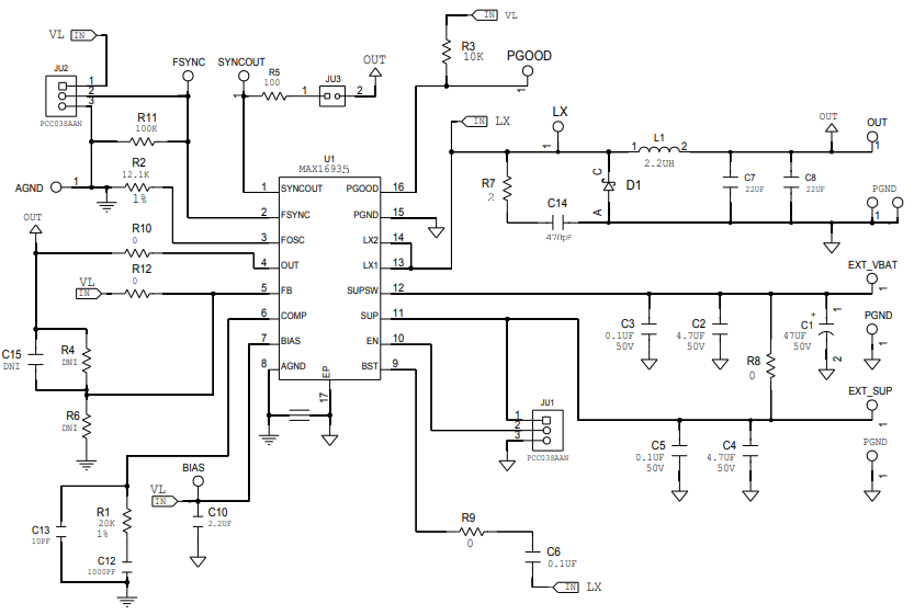
EVKIT link: https://datasheets.maximintegrated.com/en/ds/MAX16935EVKIT.pdf
***END OF PART 3
**************************************************************************************************************************
PART 4
LED Drive - Features and Specifications
As mentioned in earlier parts, the LED Driver specs can be summarized as follows:
- 2 Channel
- 10A maximum total continuous current
- 12V working voltage for 12V LEDs
- Standalone LED current limiting feature
- PWM brightness control
I won't be using specific LED driver IC's in this case and will just implement a PWM drive to allow brightness control and current control. The supply is already specified to be of a 12V rail and thus no need for a dc-dc conversion step. This will simplify the setup as a whole.
LED Drive - Schematic
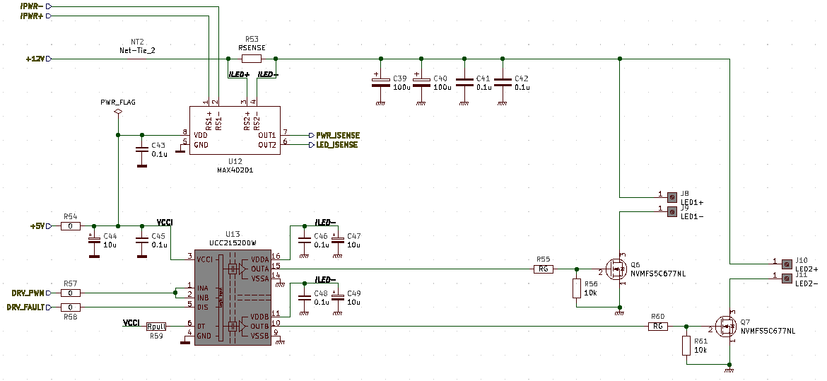
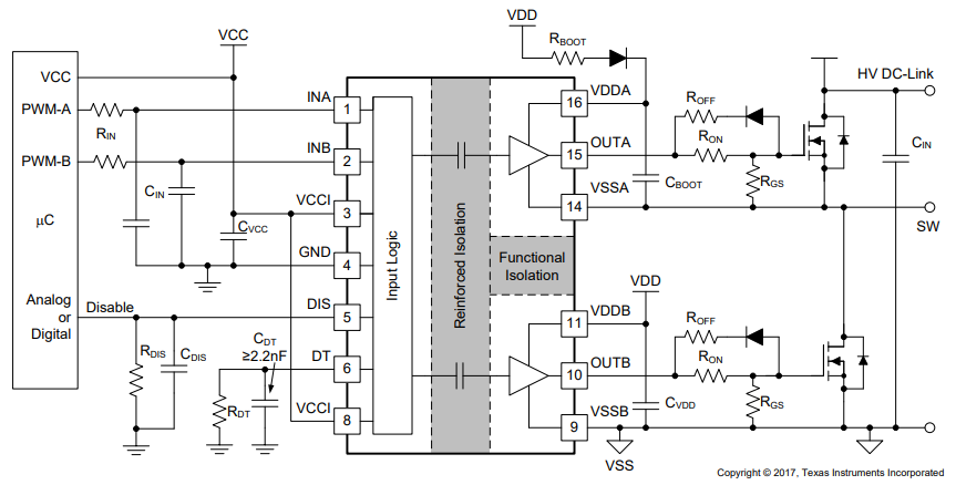
For a 2 channel implementation, I will be using a universal gate driver from TI that is capable of dual low side, dual high side, and half bridge configuration: UCC21520. For this case, a dual low side implementation will be used to drive 2 channels of the LED connection. The said IC is a little bit on the high end spectrum as it is more suited for high frequency operation, up to 5MHz, and can drive SiC MOSFETs that can take advantage of the isolation from input to output when implementing a negative gate drive. I used it in my previous project so I happen to have a few of them left, and so I decided to use the remaining pieces.
UCC21520 Datasheet: http://www.ti.com/lit/ds/symlink/ucc21520.pdf
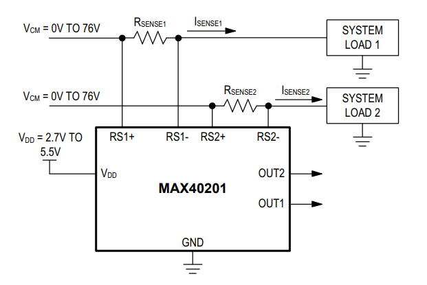
The current sensing block features Maxim's MAX40201 Dual-Channel, 0V to 76V Current-Sense Amplifier. Channel 1 of the device is used to sense the overall current consumed by the whole circuit and triggers the OCP feature discussed in the Power Section. Channel 2 provides current monitoring of the LED Drive section, which will enable the system to isolate the LED current consumption from other parts of the circuit. The current sensed from channel 2 will be fed to the system's controller for LED monitoring purposes. The high side sensing configuration allows no disruption of ground return currents compared to current sensing approaches implemented at low side. The high side configuration can also take advantage of the bypass capacitors that allows filtering of the current sense signal. The specific device I have available features a 50V/V gain in an 8pin uMAX package.
MAX40201 Datasheet: https://datasheets.maximintegrated.com/en/ds/MAX40201.pdf
LED Drive - Components and Design Resources
The N-Channel MOSFETs used are both rated at 36A and 60Vds. The RSENSE resistor is a 5mOhm SMD chip type capable of sensing up to 20A of current.
The current sensing configuration is based on the following diagram:
While the Gate driver configuration is based on the diagram below, modified for dual low side implementation:
***END OF PART 4
**************************************************************************************************************************
Conclusion:
This ends part 3 and 4 of this project series. Part 5 will discuss the connections of other peripheral blocks to the microcontroller. Hope this documentation will help other makers out there. Don't forget to leave your feedbacks in the comment section. Thank you!