There is a problem with the layout of the current sense circuit that distorts the ‘B’ side signal. Here is a trace:
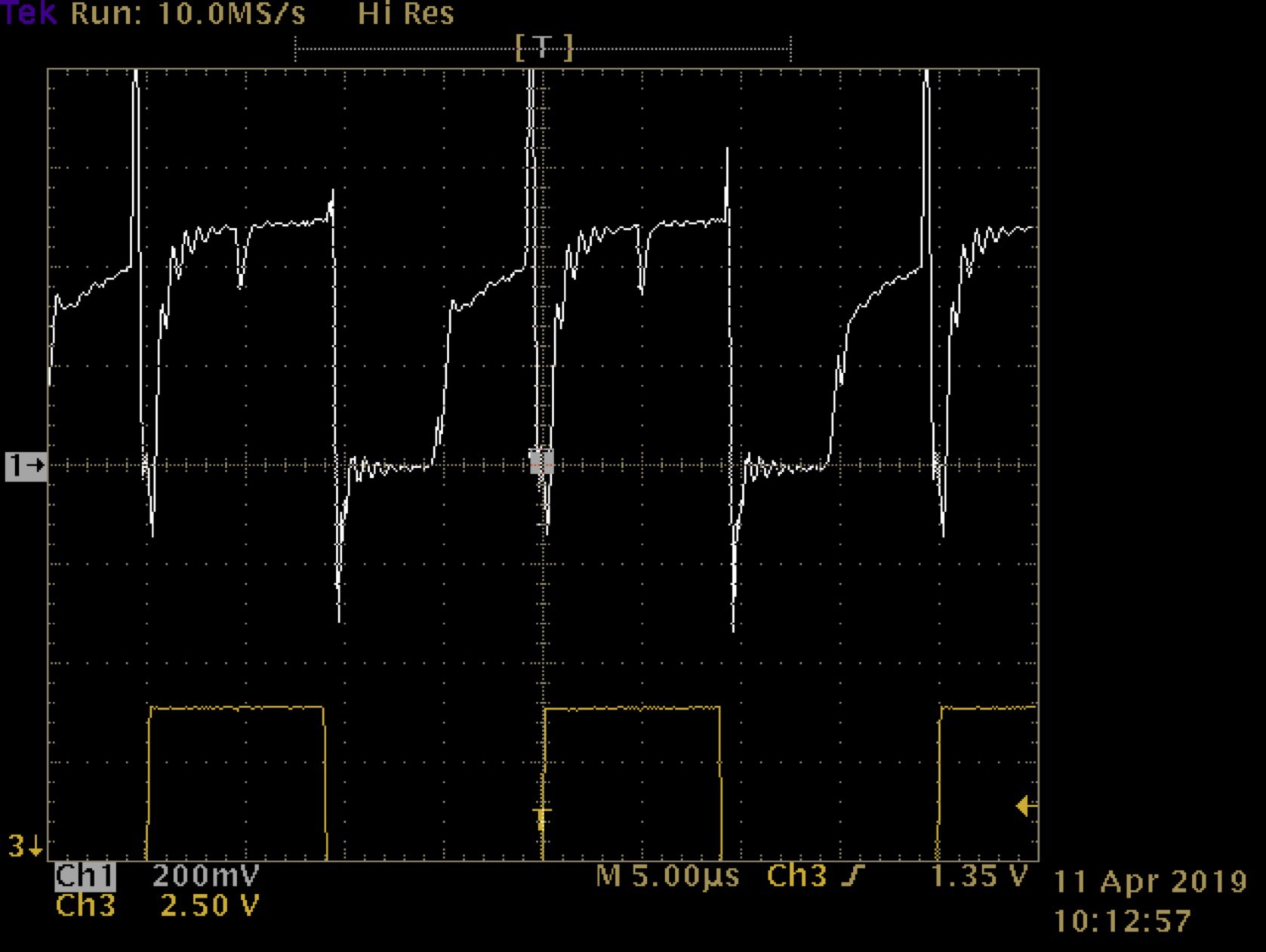
Channel 1 is the sense signal at the gate driver card pin connecting to the main board. Channel 3 is the ‘A’ side drive signal, so when 3 is low the sense signal is coming from the ‘B’ side of the bridge. Amazingly, it doesn’t appear to effect the safe operation of the unit. Below is a trace of over-current limiting prompted by a surge event on the sine output:
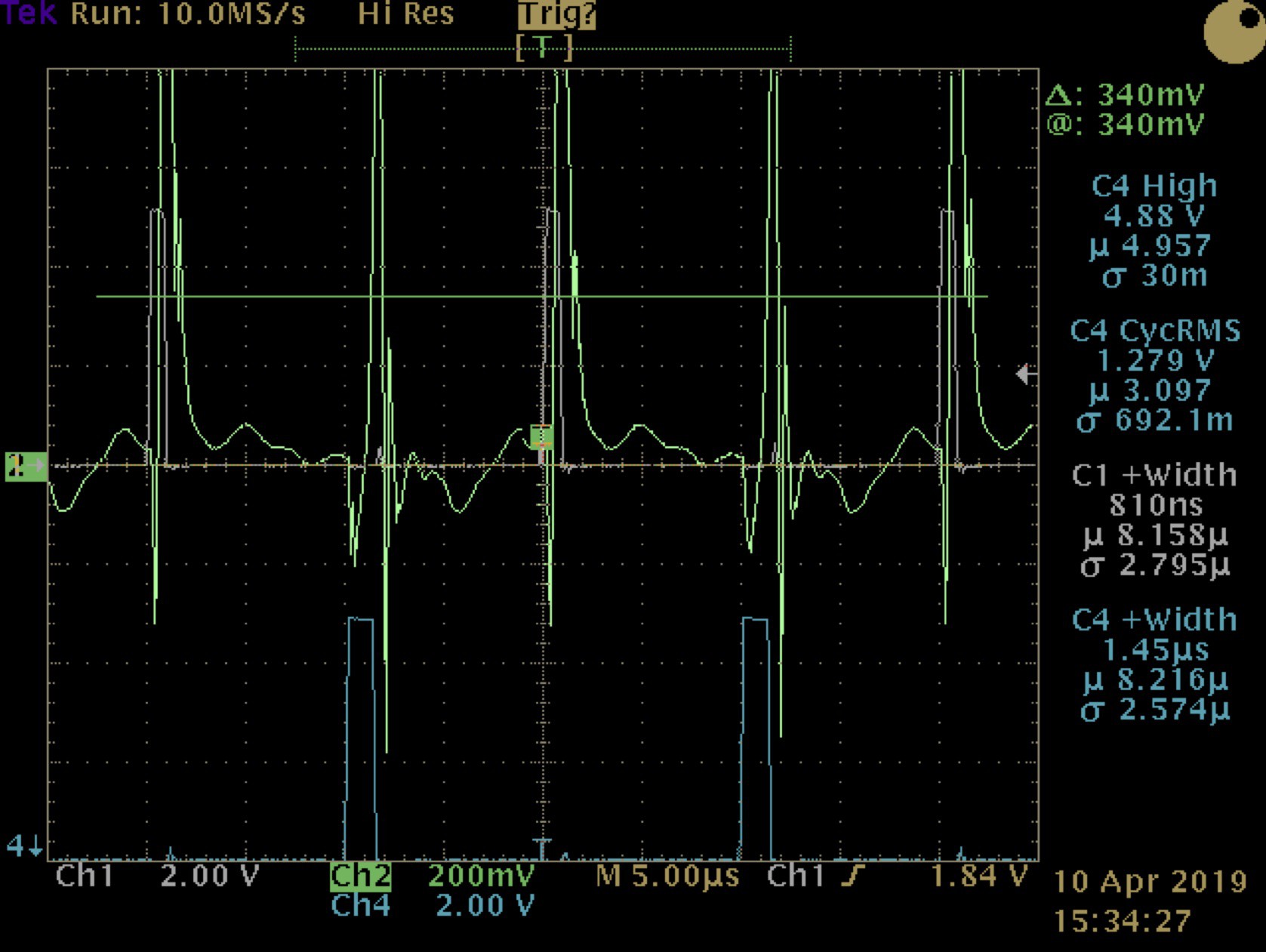
Channel 1 is the gate drive for the ‘A’ side and channel 4 is ‘B’. Channel 2 is the current sense signal from the gate card pin. Note the delay and subsequent higher DC for the ‘B’ side; but still short enough to protect the transistors.
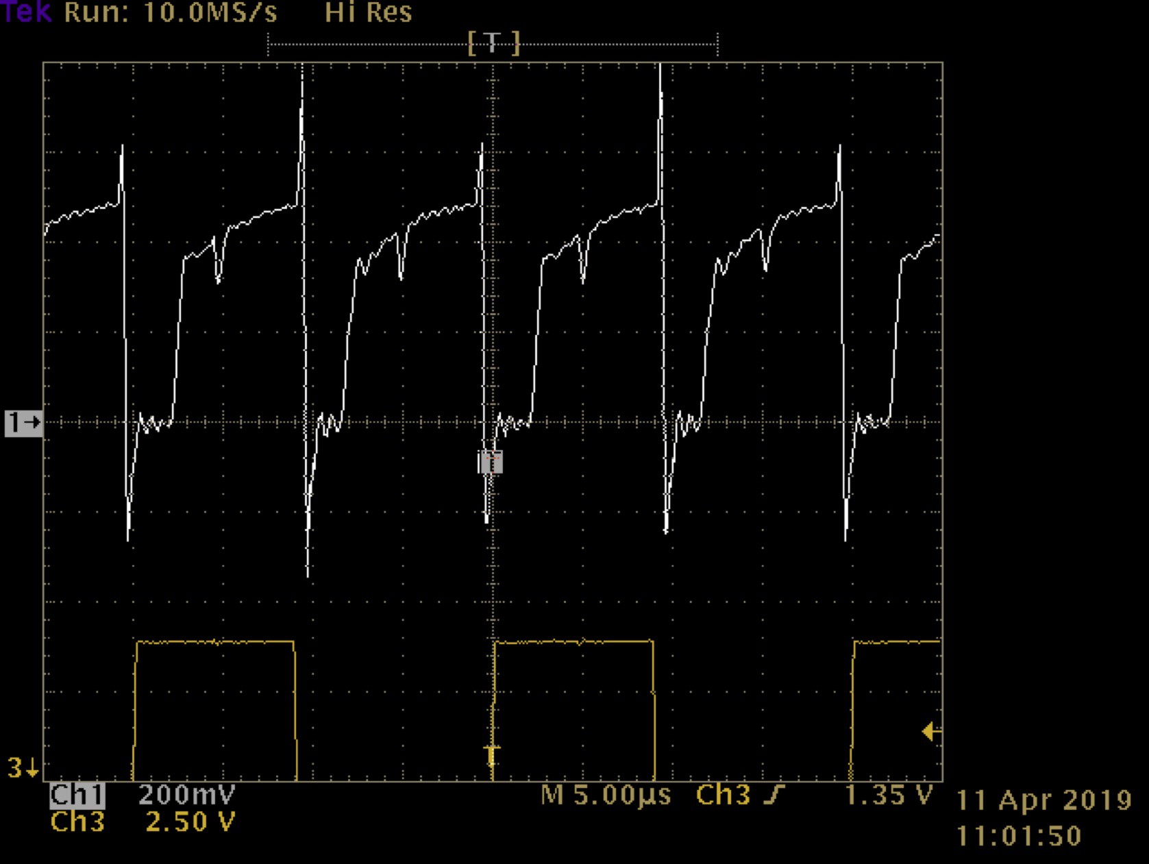
Instruction ten describes a fix to improve the B signal and it’s highly recommended that you do this. Below is the output from the sense pin with the modification.
So what happened? Poor layout is to blame: the circulating currents in the bridge traces interfere with the signal. Using discrete wires avoids this.
A proper fix requires placing the amplifier closer to the sense resistors and at the same time keeping the distance from the amplifier output to the controller short as well. As explained in the log on the general design problem that is essentially a redesign.
Discussions
Become a Hackaday.io Member
Create an account to leave a comment. Already have an account? Log In.