In other logs I’ve written about how specific aspects of the controller design integrate with the hardware so this one explains the architecture in more detail.
Overview
The controller is a Microchip PIC16F1776 8-bit microcontroller (MCU) with 16KB of flash program memory and 1KB of static RAM. The system oscillator is set to 16MHz with an instruction speed of 4MHz. The firmware is written in ANSI C and compiled in ‘Pro’ mode using the XC8 compiler.
On-board peripherals handle all real-time control (bridge, current protection, ADC, etc.) so, the MCU’s 4 MIPS is adequate and the firmware uses a polled architecture. Its main job is to provide operating envelope management and communicate status via the front panel LEDs or service port.
Most of the source code is well documented and supplements what’s presented here. You’ll notice that the compiled code size is large - this is to support the console interface.
Boot Process
The boot process is divided into three stages:
- NVM / CPU validation
- Peripheral configuration
- Inverter startup
At boot the Power Control (PCON) and CPU status (STATUS) registers are evaluated to determine if the boot was due to a watchdog or CPU trap (e.g. stack). If any of these conditions evaluate TRUE the boot will complete with error and a status code set on the front panel LEDs. The inverter will not start without power cycling which is done for safety.
A row of program flash is used to store the system configuration and the last word contains the checksum for the row. This value is compared to the dynamically generated checksum. Similarly, a mismatch causes the boot to complete with error, set an LED status code, and prevent normal startup without power cycling.
In both of the above situations the status code will be written to NVM. In the case of the checksum error this has a self healing effect: the entire row is rewritten with default values which should reset the checksum unless there’s a flash memory failure. Also, while the inverter won’t start, the service port is active and can be used to troubleshoot.
The second boot step is peripheral configuration. This starts with loading configurable parameters from NVM and then configuring the on-board peripherals. No validations are performed during this step.
Inverter startup is performed in the run-time loop. Once the data collection block validates the operating environment (e.g. temp, current, voltages), control proceeds to the boot (autostart) block. The NVM configuration directs what happens: the unit can remain stopped, start only the inverter section, or start inverter & sine sections. When the inverter is started several things happen:
- The bootstrap capacitors are charged. High-side shorts are also detected.
- A soft-start function slowly increases the duty cycle from 0 to the set value to reduce component stress and EMI.
- The steady state duty cycle is monitored to detect shorts (or other HW malfunctions that would reduce duty cycle).
If NVM also directs the sine section to start then the sine command pin (PIN_O_SINE) is asserted and the acknowledgment pin (PIN_I_SINE) is monitored to confirm start within the timeout period.
Any error encountered during startup sets the unit to a stopped state with the front panel LEDs displaying an error code. A power cycle is required to restart.
Run Loop
The run loop is a waterfall design and consists of several discrete conditional sections that execute sequentially:
- Watchdog timer: this is reset at the top of the loop.
- Data collection: system voltages, temperatures, and current. Many of these are averaged over several samples to eliminate noise and ripple. These values are used in subsequent processing blocks.
- Thermal management: turns fans on & off based on inverter temperature and thresholds set in NVM. A ‘feature’ of this block is that it can be used to measure the execution time of the control loop. This is done by setting a higher off temperature than on and measuring the duty cycle at the fan power pin. Best to do this with the fans disconnected.
- Run-time control: provides envelope protection and disables the unit if voltage, current, temperature, or power limits are exceeded. Some evaluations, like an input over-volt condition, require immediate shutdown. Others, like excessive power uptake, must be tolerated for short time periods to accommodate the operating requirements of connected equipment. These parameters are employ a simple Proportional-Derivative algorithm.
- Boot (or autostart): previously discussed.
- NVM status recording: most error codes that cause the MCU to shutdown the unit are recorded for troubleshooting.
- LED display: sets the front panel LEDs to display a status code or load in 25% increments.
- Console monitor: similar to the Unix ‘top’ command, this outputs various system values to the service port at one second intervals.
- Console service: processes commands entered via the console.
NVM Storage
The MCU’s flash program memory is arranged in rows of 32 words. A row is reserved for storage of configurable parameters by defining an array of constant unsigned characters. Only the lower byte in each word is used for data since the memory cells of the upper byte only contain six bits. The compiler knows this and will only utilize the low byte.
The last two bytes of the array are reserved for the checksum which is calculated by summing bytes 0-29. The flash architecture requires that to write a new value to any byte in the row the entire row must be erased & rewritten.
NVM is updated via three pathways:
- Checksum error - previously covered in boot discussion.
- Console command that updates an NVM value. NVM is updated as part of the console routine processing the command.
- Error status code. Abnormal conditions detected by the MCU will cause it to shutdown the inverter and set an error code. All error codes except under-volt-lockout (because it happens when the unit is turned off and are considered an expected error) are recorded in NVM. Precautions are taken to ensure that Vcc is high enough so that even if the unit has lost power, the Vcc hold-up time is sufficient to allow the erase & write cycle to complete without corrupting NVM. Note that only the last status code is written to NVM and, since there’s no real-time clock function, does not include a time stamp.
Interrupts
The polled architecture eliminates the need for interrupts with two exceptions. A system timer (TMR8) is used as a rudimentary chronological countdown timer, primarily for the console monitor function. Second, the USART peripheral generates an interrupt when data is received.
Data Acquisition
With the exception of the COG timing (Complementary Output Generator) all data acquisition is performed by the 10-bit ADC peripheral. An abstraction function, ReadVoltage, manages the ADC hardware interface and allows the firmware to select the analog channel and convert the result to an object of type volts. The ADC’s Vref is the internal 4V reference so no calibration is necessary. The raw ADC value is stored along with the scaled voltage and modulus (mV). The volts & mV are also stored as a composite value in an unsigned 16-bit integer. The 10K/1K places are reserved for volts and the 100/10/1 place for mV. So 3.74 volts would be stored as 3740.
All of this is clunky and imposes a lot of overhead on a processor with no multiply/divide ALU, so why?
- It’s an outgrowth of development from its predecessors where a human interface to display what’s going on was necessary.
- The overhead isn’t so bad that it impedes the controller’s function or presents a safety hazard.
- Given 1 & 2, I don’t want to invest the time to clean it up!
The duty cycle of the COG (bridge) is measured using Timer5 with the gate control feature. This allows the timer to be cleared and triggered by the assertion of one of the COG pins. Timing ends when the COG pin clears. Since both the COG & timer are referenced to the same clock it provides a very accurate on-time value. The function that measures this is blocking - meaning that foreground controller execution is paused while timing. This comes out to just over 10uS. The function is written to abandon timing beyond this to prevent a hung state that would result in a watchdog reset.
COG timing is vital to the over-current protection function since it looks at this value to determine if hardware current limiting is engaged (the DC will be substantially reduced). Like the ADC composite voltage this is an odd approach: the ‘normal’ way for firmware to trap over-current events is to have the comparator trigger an interrupt which in turn sets a flag or increments a counter that the foreground code can monitor. In this design the noise on the current sense line at the end of a cycle is substantial and creates many interrupts. And, unlike the COG feature to ignore falling events (blanking time), this can’t be done with interrupts. Hence, the rapid fire of interrupts causes the MCU to reset. Some will argue that this is compensation for a poor hardware design and there is merit. I would counter that his solution allows for a simple, and cheap, design without compromising reliability or safety, although EMI may be another matter.
Service Port
The service port is a micro-USB plug that provides a TTL level RS232 interface and the ability to update the firmware using Microchip’s PICkit 3.
The port follows the USB standard for power so that if someone accidentally plugged in a charger it should not, in theory, damage the controller (I have not tested this).
The RS232 interface provides a simple console interface to configure & control the unit’s operation. This includes starting & stopping the unit and setting NVM values. The interface runs at 115.2Kbps, 8 data bits, 1 stop, no parity, and no flow control. The RS232 service routine uses the new line (0x0A) character to terminate a command line and also recognizes the backspace (0x08) as destructive.
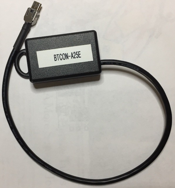
To connect to the console I built-up a bluetooth adapter I call BTCON. It’s another project I have posted.
Command Set
The command set utilizes two characters and many require a single parameter. The first character of the command defines its group - like ’S’ for Set or ’T’ for Temperature. The help, response, and status displays can be a bit cryptic - that is done to conserve program space. To help, many of the status responses use the command value as the prefix for the field.
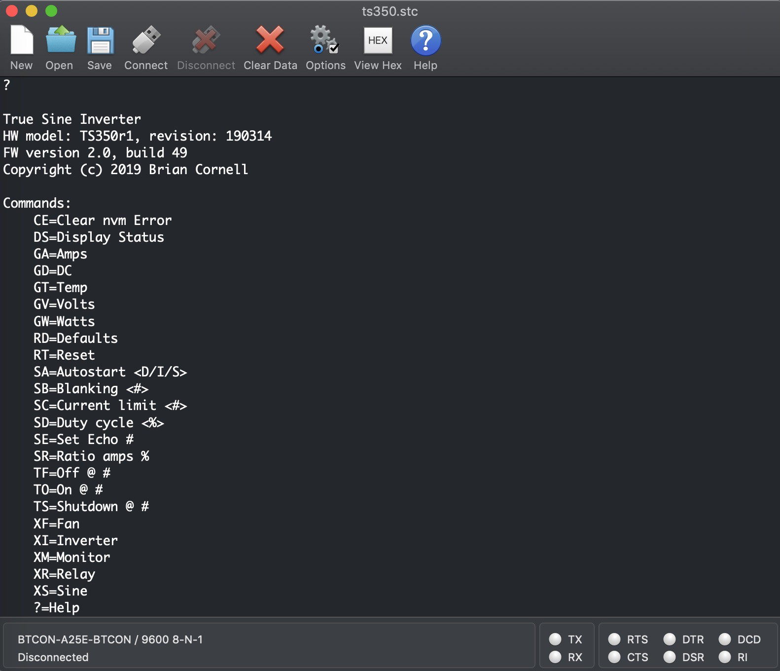
Below is an explanation of each command. You can get this list by typing a question mark (?) and pressing ENTER too. Be sure you know what you’re doing before changing values - the unit could easily be destroyed with an improper setting.
Miscellaneous commands.
CE Clear nvm Error.
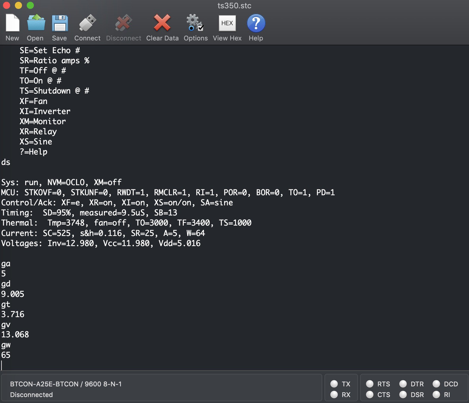
DS Display Status. Displays all configurable parameters along with all acquired data and the unit’s operating state.
The Get commands are taken from GPIB syntax in that the response only contains the value to make consumption by a data collector easier.
GA Amps. Returns an integer representing the averaged input current.
GD DC. Returns the duty cycle in uS.
GT Temp. Returns the voltage of the inverter’s NTC. Refer to the thermal tab in the design workbook to get the temperature.
GV Volts. Returns the inverter’s input voltage.
GW Watts. Returns the inverter’s input wattage (load).
Reset commands.
RD Defaults. Reset NVM values to defaults.
RT Reset. Reboot the MCU.
Set commands update real-time and NVM.
SA Autostart <D/I/S>. Set autostart to Disabled, Inverter only, or Sine (includes Inverter).
SB Blanking <#>. The amount of time that COG falling events are blanked (ignored). Multiply this value by the system oscillator period to obtain the time.
SC Current limit <#>. The maximum current, represented as a voltage, before current limiting begins. The valued entered here is the DAC value - not the actual voltage. To calculate the voltage: (#/1024)*4.096. Using the default of 525 gives 2.1 volts. To know how many amps this is divide by 15mV, so 2.1/0.015 = 140. That’s not a typo - 140 amps! So be careful if you think you need to increase this value.
SD Duty cycle <%>. Sets the duty cycle in percent. Enter a value between 5-95.
SE Set Echo #. Sets character echo off when #=0. Any other character sets on.
SR Ratio amps %. Reduces the current read from the S&H circuit by % percent to obtain a first order approximation of RMS. Refer to the Current Monitoring and Over-Current Protection log for a technical explanation.
Temperature commands update real-time and NVM.
TF Off @ #. Turns fans off at # temperature where #=the composite voltage of the inverter NTC. The default of 3400=3.4V or ~ 36C
TO On @ #. Turns fans on at # temperature where #=the composite voltage of the inverter NTC. The default of 3000=3.4V or ~ 45C.
TS Shutdown @ #. Shuts the inverter off at # temperature where #=the composite voltage of the inverter NTC. The default of 1000=1.0V or ~ 92C.
Toggle commands echo their on/off status when executed.
XF Fan. Disable / enable. Use with care.
XI Inverter. On or off. If Sine is on and inverter is turned off sine is stopped first.
XM Monitor. On or off.
XR Relay. On or off. If the unit is under load and the relay is turned off the start circuit fuse will likely open.
XS Sine. On or off.
Peripheral Propagation Delay Considerations
In early testing I had an odd and seemingly random problem where one side of the bridge would miss a complete cycle. It only appeared when the duty cycle was above 92% or so. That should have been my clue but I ignored it and spent a lot of time chasing phantoms - current sense, gate drive, transformer saturation, etc. Finally I came back to that and studied the current sense timing. Remember all that noise on the sense line at the end of a cycle I’ve talked about?
Turns out that noise ring has a duration just over 500nS so, when the DC is at 9.5uS it is still present at the start of the next cycle. The COG’s FE (falling event) configuration was to trip on a logic low from the comparator. Look at the logic diagram in the Current Monitoring and Over-Current Protection log. Theoretically PWM11’s output should be high and hence CLC3 should have prevented propagation of the low state from CM2. The problem was the propagation delay from PWM5->PWM11->CLC3. I didn’t bother to measure it and would guess its probably on the order of 10nS or less but it was enough.
The fix? Change the COG’s FE mode from logic low to state transition. Once more the MCU’s flexibility bailed me out. The real lesson here is to never ignore noise & rings as they will burn you in myriad ways no matter the innocence or ways you find around them. Also, don’t forget to pay attention to on-chip propagation delays.
Discussions
Become a Hackaday.io Member
Create an account to leave a comment. Already have an account? Log In.