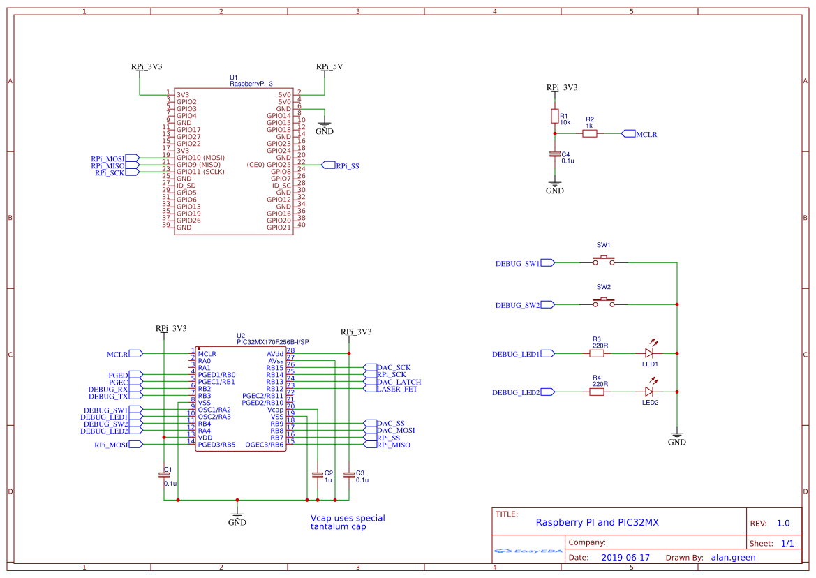
Following on from last posts' high level design, I drew up schematics. I like to keep each part of the schematic down to about one A4 page, so I can easily print it all.
These schematics represent a point in time. The will change as the project goes on. When I'm finished I'll upload them in full.
Voltage Shifter
The voltage shifter takes the DAC_X and DAC_Y signals, and turns each into a differential pair suitable for input to the galvos.

Based on my experiments with the signal generator, I don't need the full galvo deflection range, so I decided to go for an +/-8V differential range rather than the full, standard +/-10V range.
Generating the signal is two step process:
- We take the DAC's output range of 0-2V, and map it over the range 4V to -4V using one op amp. I
- We then find the inverse of that signal by using an op amp in standard inverting buffer configuration.
In step 1, we map the DAC's range somewhat upside down, by mapping 0V to 4V rather than -4V. The reason for this is that the op-amp configuration is more straight forward this way. Since we are always going to need both the positive and negative signal, it doesn't matter at all which we calculate first.
I used the site earmark.net to understand the required amp configuration and calculate resistor values. Bruce Carter has been extraordinarily generous in providing this resource.
[Parenthetic note: the DAC's actual range is 0.01 to 2.048V, but using 0-2V significantly simplifies the selection of values. I'm using 1% resistors, so the error from this simplification is much less than the accumulated error from other sources.]
MCUs
The PIC32 has some requirements, handily documented in section 2 of its datasheet. At least we don't need an external clock crystal. The Raspberry Pi comes with all its own support circuitry and the schematic just shows the Frame Driver's connections to the RPi's I/O header.

In addition to the usual bypass caps, the PIC32 requires:
- a small reset circuit,
- an expensive 1uF tantalum capacitor on Vcap to stabilize the internal LDO power supply.
There are also a couple of buttons and LEDs for debugging purposes.
(Looking at the schematic, I can see I'll likely want to add a reset push button, too. )
DAC and MOSFET
These are devices the PIC32 sends commands to, in order to drive the galvos and laser.

We power the DAC from a special 3V3 supply (3V3Ref) to help ensure the stability of its internal voltage reference. 3V3Ref is also shared by the voltage shifter.
The DMN2046U N-channel MOSFET controls power to the laser. Because the FET has ~300pF of capacitance, there's a 100Ω resistor inline on the LASER_FET output pin to reduce maximum output current to a peak of about 33mA - which is still twice the "maximum allowed" of 15mA. (Interesting discussion about gate resistors on Stack Exchange.)
Power
In previous projects, I've been bitten hard by noisy power supplies. This is likely overkill, but I'll start from here and then maybe experiment with removing some of it.

I am using an 7808 and 7908 to generate +/-8V from the galvo's +/-15V supply. The values of capacitors were taken from the datasheets, but I don't think they're particularly critical. The +/-8V is used to power the op-amps. While the op-amps can happily use +/-15V, its not clear to me that the power supply would be clean enough, especially when the galvos are under high load.
3V3Ref is generated from the RPI's 5V supply. It's purpose is to be a clean 3V3 supply for the DAC and to be used as a reference by the op amps.
Next steps: soldering!
 Alan Green
Discussions
Become a Hackaday.io Member
Create an account to leave a comment. Already have an account? Log In.