 John Lonergan
So the project is still in the simulation phase and it's not a long way from the original very simple SPAM-1 idea.
I'm still learning a lot about verilog and will probably do a piece/video on some of the things I've learned along the way.
This project started as a very simple CPU design, but as I got into it and finished the simulations and was about to build I felt that building something so trivial wasn't going to be worth it and I needed something that was more of a challenge.
I wanted to try something that had a more capable ALU for starters and also wanted to be able to some more sohpisticated things like direct and register addressing of the RAM and ROM.
Around that time I got talking to Warren Toomey about borrowing his ROM based ALU design and Warren suggested I commit any design to verilog to test it out and so that journey began.
I'm actually on the third design iteration. The original as mentioned was too simple. The second was a lot more complicated but despite the additional complexity it still lacked a lot of capabilities that I thought and half reasonable CPU would support, so I felt the complexity wasn't justified. So rather than making it simpler I decided to make it a little bit more complex, but in the process made the CPU capable of funcitons that justified a bunch of complexity.
I've now spent months getting to grips with verilog and have now created what's probably novice level unidiomatic verilog code for all the physical components I'm using plus a few that I'm not.
In most cases I had to create or modify existing 74xx verilog components that I found on the internet because the ones I found were not accurate in terms of pin-out or function vs. the physical chips. For example, I found various dual port RAM models in verilog but the physical stuff is a single port RAM with tristate outputs. I found this all pretty surprising. Additionally, I found that a lot of verilog chip models seemed to lack the relevant propagation delays, so I've spent ages sorting that out too. I think this lack of faithfulness to the physical devices may be because a lot of these existing efforts are intended to be used to burn an FPGA implementation and not to build using discrete devices.
So in github I now have a small library containing a subset of the 7400 chips plus ROM , RAM amd UART that are all wired and timed as close to the real thing as I can be bothered to make them; hopefully someone else will find this stuff useful.
This detail was necessary given that the whole point for me of this effort was to achieve an accurate simulation of the CPU including all timing delays so that I could hope to spot errors and glitches before committing to hardware.
So the beastie I'm trying to implement is shown in the image below.
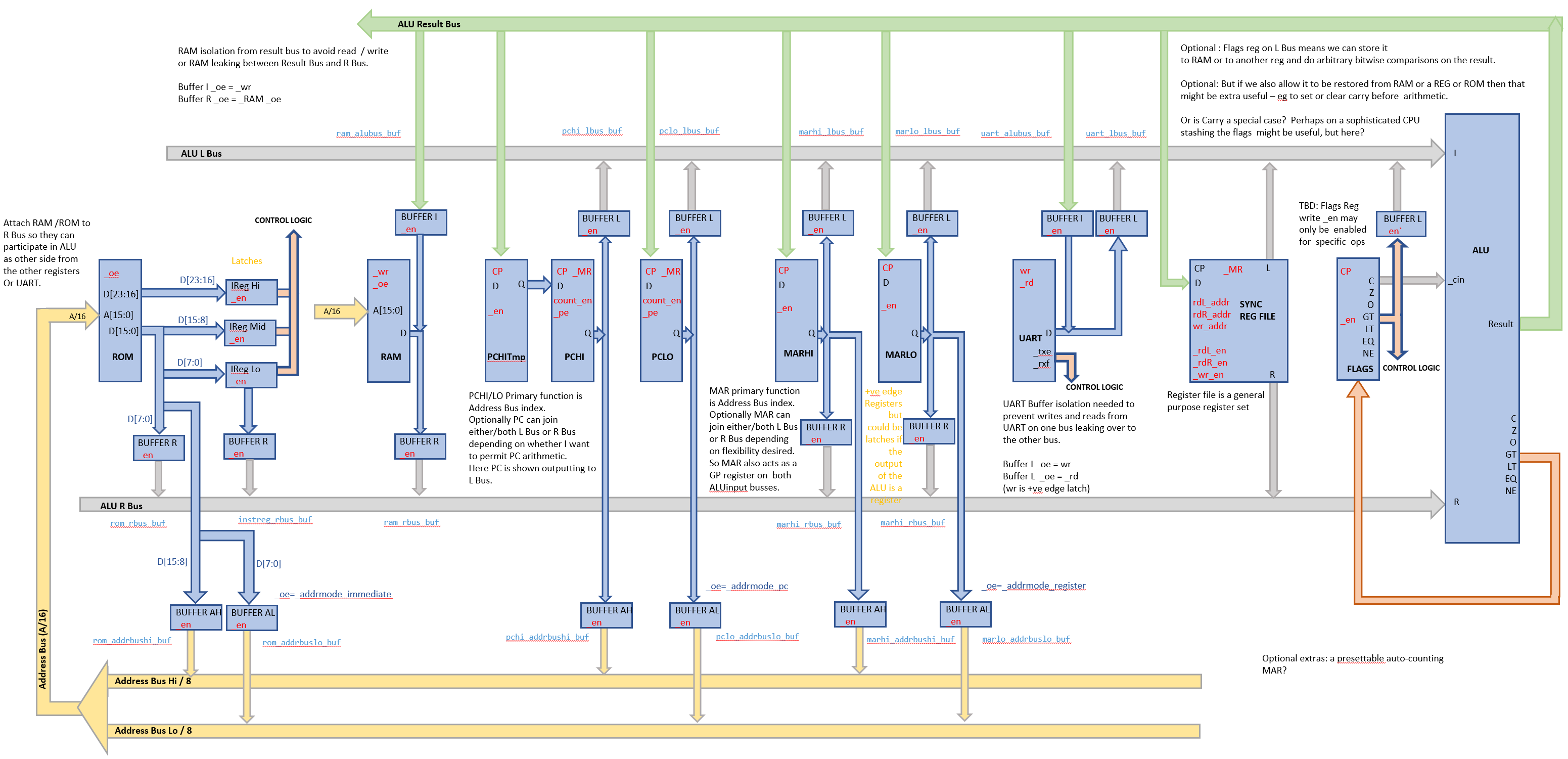
There's an 8 bit ALU which has "left" and "right" input buses for the arguments; everything goes via the ALU.
There are a bunch of devices, including the ROM, RAM, UART, memory address registers, PC and a small register file that can optionally output onto either the left or right ALU input bus. The output of the ALU feeds back into these devices.
I might not implement all these options in hardware. For instance in the design above the two MAR registers can act as general purpose registers due their participation as inputs to the ALU. However, I decide not to bother allowing the MAR to feed into the ALU on either or both channels. Also, likewise perhaps I won't bother allowing read access to the PC. Also, I show the flags register as potentially being an ALU input; also only an option. However, there's an initial core I will definitely build.
The register file is build using a pair of 74HC670's (4x4bit reg files). I wanted to find a place for these async chips out of curiosity, but the other registers like the MAR are regular 8 bit +ve edge registers. The async nature of the 74HC670's adds some complexity but since this is all an experiment and learning exercise I'm not too bothered about that and I've put a synchronous register on the data in to the register file to prevent feedback loops through the ALU.
But anyway, I've now got a simulated design now that lends itself to incremental extension, where I can get a simple functioning CPU together and then extend it gradually in various directions to ultimately end up with the full blown thing below if I have the stamina.
This looks like quite a challenge to me, and having written the control logic in verilog I know it's going to be a mess of wires.
The design effectively has 4 or 5 busses and given this is being built on bread board I'm probablyt going to use ribbon cable for the bus rather than use the power strips as I've seen other do.
I'm going to give it a try anyway - and find out if this effort leaves me any time with the family at all - or drives me insane.
The instruction set is really designed around the idea that all ops really do is move data from one place to another and perhaps transform is along the way, and I've crammed these into 24 bits. I've just going to use three roms for this nothing too clever.
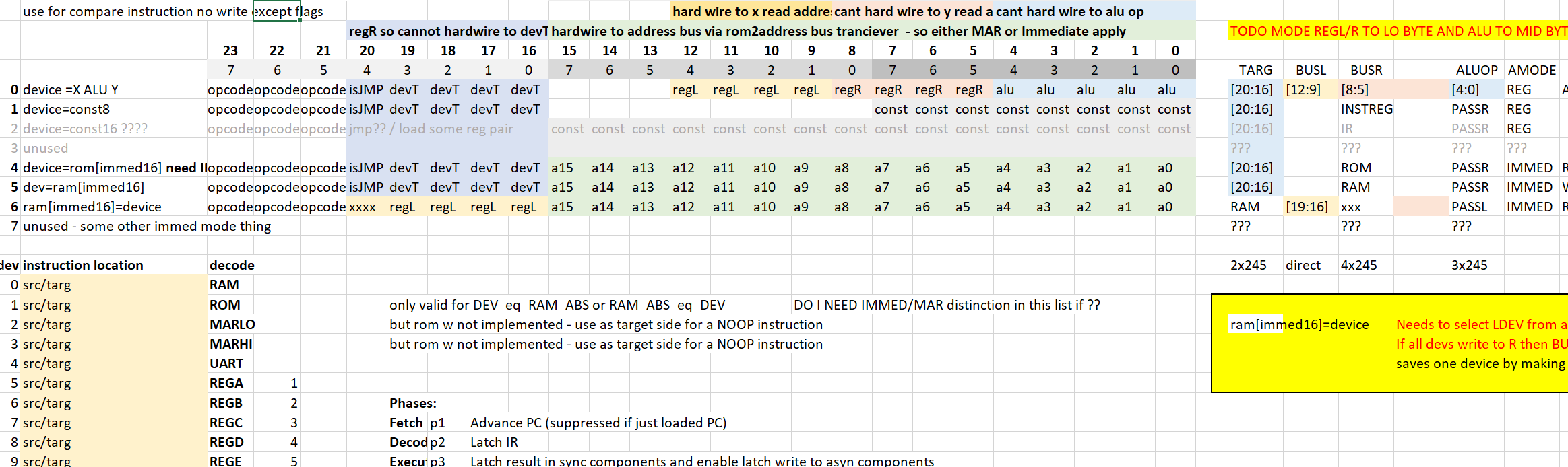
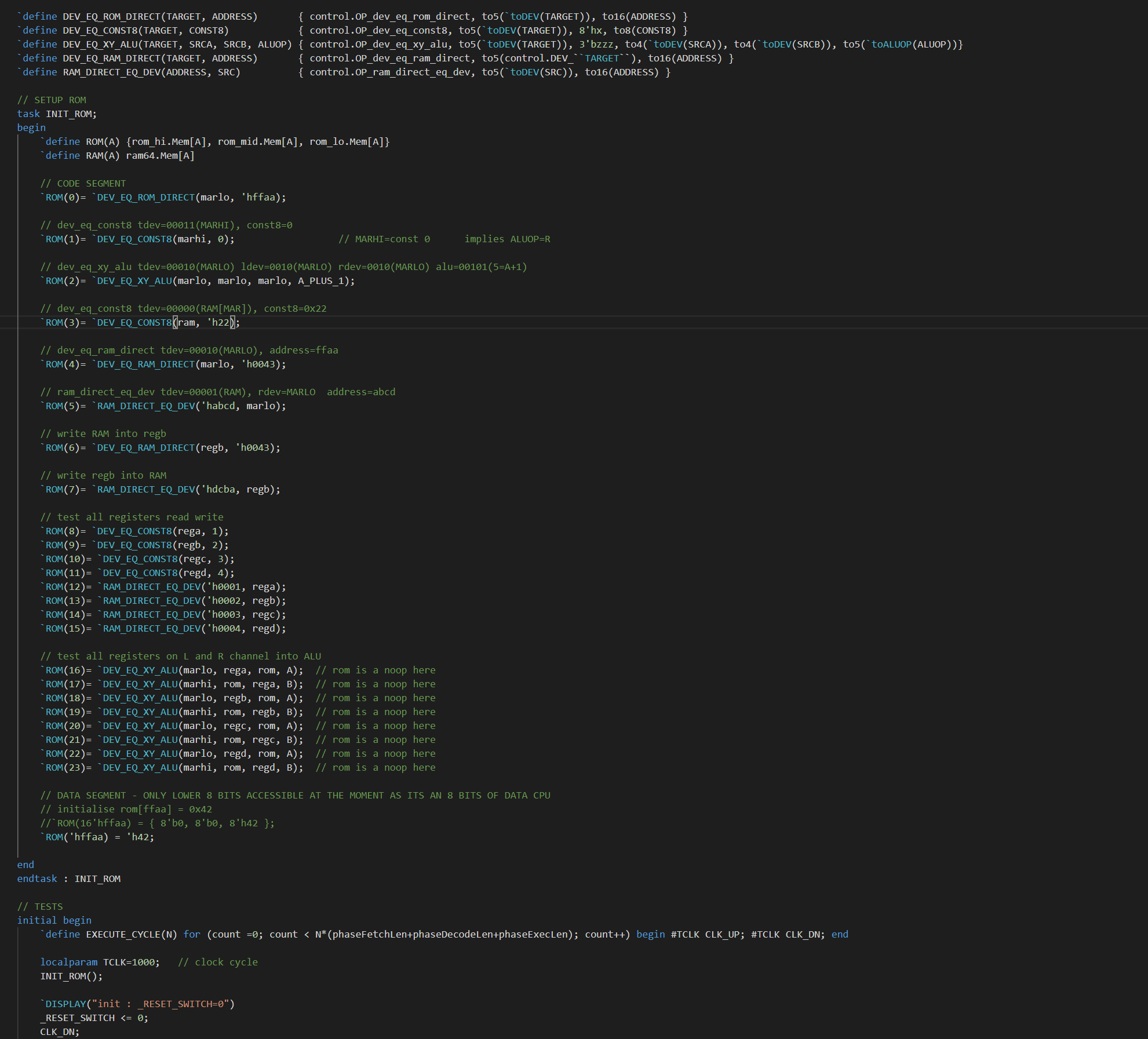
There are only 5 instructions and in the verilog I've created a kind of pseudo-assembler in the tests ...
Along the way I've also come up with curiosities like an interactive Verilog UART implementationt that reasonably closely honours the UM245R behaviour. That was pretty interesting.
So tonight I plumbed in one of the last components, the register file. I've decided to use diode logic to the control lines into this component just for the experience. Not sure it will save any space but it may be interesting to use multuiple techniques.
I think the last two things I have to add are the flags register and the jump logic.
That will probably take a few more evenings.
Then I have to find a space in the house where my wife will let me make a huge mess of wires.
Discussions
Become a Hackaday.io Member
Create an account to leave a comment. Already have an account? Log In.