In between work on the balancer I've been considering topologies for the charger. So much depends on the panel configuration and working voltage. Within the charger, higher voltages correlate with higher efficiencies because of lower currents. This is even more important with a homebrew design where heavy-weight PCB costs are prohibitive and inductor / transformer fabrication capabilities are limited.
The TS350 project provided many lessons on the limits of power, efficiency, and transformer design with low input voltages that I want to avoid repeating. I settled on 500 watts with a nominal 60-65V input. Two 270W, 31.4V, panels in series would power the charger and deliver 540W at peak MPP. Of course these are perfect condition numbers that will [likely] never be obtained. Further, it requires the charger to have a minimum 92.6% efficiency (500/540). With an input current of 8.6 amps RMS this could prove challenging.
Here's the I-V curve for the panel I'm considering. A lot of energy is left on the table if the charger isn't able to boost the panel voltage to that of the stack.
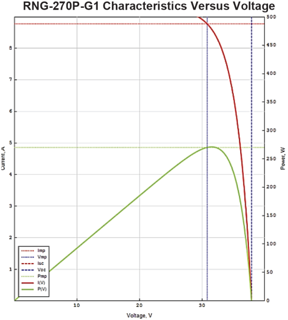
Even at 10 volts there's better than 90W available. With two panels in series there will be 180W @ 20V. So I need a topology that can handle open circuit voltages in excess of 80V and capable of boost to at least 20V and preferably 10V.
Another key criteria I have is to minimize input current ripple since the panels will probably be located several meters away from the charger and high frequency ripple generates copious EMI and increased losses in the supply wiring. For example, a pair of 10AWG wire ten meters in length with 3mm lead spacing has ~ 3.36uH of inductance. To limit the voltage noise to 50mV with a ripple current of 1A would require 5,400uF of bulk capacitance. Output current ripple isn't as much of a concern since the charger will be located close to the battery stack and they are essentially a very large super capacitor.
Last, I prefer the power stage to be as simple as possible: defined by a minimum of switching and inductive elements since these incur most of the efficiency loss.
So far the design criteria are:- Output voltage=56V
- Output power=500W
- Output current=9A
- Efficiency=92.6%
- Nominal input voltage=63V
- Maximum input voltage=90V
- Minimum input voltage=10V
- Maximum input current=10A RMS
- Input current ripple <200mA RMS
- Simplified power section
- Isolated output not required (the battery system must be on earth ground with the panels)
As a rule I try to avoid center-tap windings on transformers. First, they are inefficient: each half winding is only active for a half cycle. Second, they waste valuable winding area and, depending on the number of turns & windings, can require a larger core size than non-CT variants. Third, the parasitic winding capacitance leads to damaging ringing on higher voltage windings: the end-end voltage is 2x the voltage applied to the half winding. This is worse for windings with a large volts-per-turn ratio. Eliminating #3 requires equipment & skills that I don't possess.
Against that backdrop I considered traditional full & half-bridge topologies. They would probably work but either require center-tap transformers or full-bridge switching. The secondary voltages aren't particularly high, but the voltage difference from end-end of the secondary will be 120V and that is close to the threshold I have found for excessive ringing on my home-built transformers. Conversely, a full-bridge rectifier on a conventional secondary creates a lot of loss.
Then there are flybacks. A non-isolated flyback won't work because it can't regulate to a lower voltage. An Isolated flyback can, but even in continuous mode they generate significant input switching ripple because the input current is discontinuous.
That sent me looking for something new. I stumbled on this current-fed full bridge topology in an ST reference design for a microinverter. It looks like a derivative of a Weinberg circuit although I can't find anything in the literature crediting it to that. In a conventional Weinberg flyback primary feeds the center tap of a push-pull transformer making it current fed. The flyback secondary can connect to either the input or output of the supply to reduce ripple current at that node.
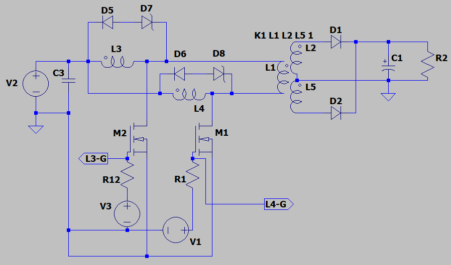
This topology simplifies both the transformer and flyback design and, like the Weinberg, has only two switching elements and is a current fed design. It is quite elegant and has many advantages:
- Input current ripple cancelation because of 180 degree phase shift in switching
- Single winding for each inductor
- Single winding primary
- Single or center-tap secondary
- Eliminates staircase saturation of transformer core
- Only two active switches
Basic operation is simple but a bit different from most bridge configurations. Inductors L3 & L4 operate in continuous conduction and, M1 & M2 switch 180 degrees out of phase and must overlap which implies a minimum duty cycle of 50%. When M2 is on L3 is charging. M1 is off and L4 is discharging thru the transformer primary (L1) & M2. Towards the end of M2's on time (depending on DC), M1 will turn on. With both M1 & M2 on the voltage across all transformer windings goes to zero. Both inductors are now charging. M2 switches off under no voltage stress and L3 discharges thru L1 & M1. This continues and the cycle repeats.
Output voltage is determined by load, duty cycle, and the transformer turns ratio. It is by nature a boost topology: the voltage the inductors impose on L1 is determined by the volt-seconds balance and hence duty cycle.
The impedance of the input inductors make it a rather bullet-proof design. And, even though I would have to use a center tap secondary I thought I could make it work for the charger by setting a step-down ratio on the transformer. It modeled well in spice at nominal voltages but didn't do well at 20V and below. It also suffers at higher voltages because it must be run discontinuous which generates more current ripple and lower efficiencies. As much as I like it I had to abandon it for this application.
Initially I put the SEPIC in the flyback bucket but decided to take a closer look (glad I did).
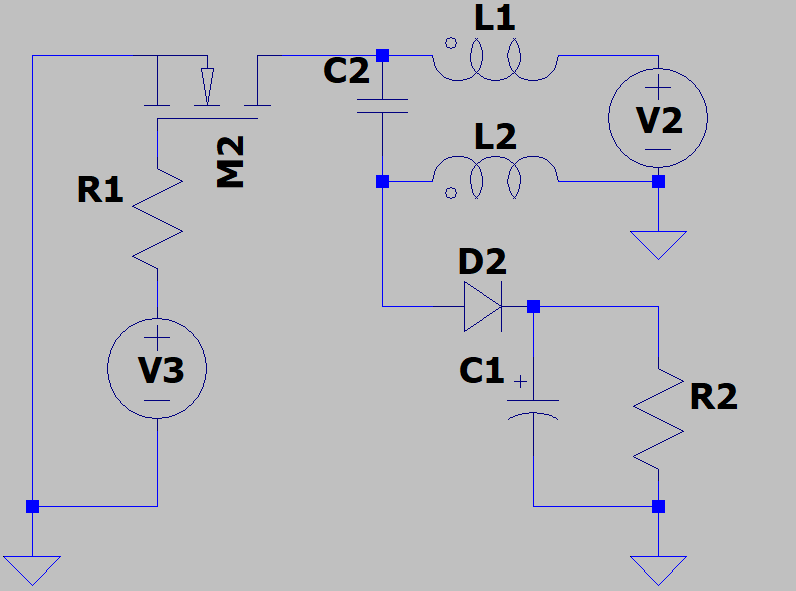
Like conventional flybacks it has only one switch - two if you replace D2 with a MOSFET for synchronous rectification. L1 & L2 can be wound on the same core and use the same number of turns which makes for a simple inductor build. Like the non-isolated flyback, L1 can run in continuous mode for a continuous input current. Best of all it can function as a buck as well as boost simply by varying duty cycle.
When the converter is first energized - before M2 begins switching - C2 charges to the input voltage (V2) thru D2 and the load (R2). When M2 turns on L1 begins charging. C2 charges L2 via M2 as well. This means voltage polarity will be negative with respect to the supply negative node but the current flow will be the same polarity as L1. While M2 is on the load is supported by C1 and there is no current flow thru D2. When M2 switches off both inductors reverse polarity by flyback action and deliver energy to C1 and the load. Energy from L1 & V2 must flow thru C2.
Since the SEPIC is still a flyback converter, the charger's power requirement will generate a significant ripple current unless the inductor value is made very large. Also, the ripple current of C2 will be larger than the output current since all energy transfer flows thru it. This is usually the limiting factor for SEPIC applications.
However, both problems can be solved by interleaving two converters that operate 180 degrees out of phase. Most input current ripple is eliminated because the triangular current ramp of each cancel. Since each converter only delivers half the power (250W), the peak currents thru C1 can be handled by paralleling MLCCs.
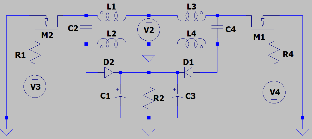
Spice simulations of the SEPIC interleave concept are promising. Full power efficiency at nominal voltage is 92.9%. D1 & D2 represent about 20W of losses and most of that can be eliminated with synchronous MOSFETs. At minimum input voltage (10V) the design delivers 90W at about 90% efficiency. Of course, this is spice and no real-world parasitics & components are modeled, but these results are promising enough to warrant prototyping.
My plan is to build a single 250W converter for evaluation. There are plenty of SEPIC controllers out there but I will use a microcontroller for better control over operation - particularly the control loop. SEPIC's have four poles in their transfer function which makes the loop harder to stabilize. And, I also have to contemplate how to balance the converters to ensure that each delivers 50% of the output.
Discussions
Become a Hackaday.io Member
Create an account to leave a comment. Already have an account? Log In.