 Eric Hertz
Times like these, it might be wise to start a new project-page, for a "subproject"... 'cause it's been so long I've actually worked on the #sdramThingZero - 133MS/s 32-bit Logic Analyzer main project, that I'mma have to read through tons of logs to remember where I left off, and to sort through TODO ideas like these...
But this idea is pretty durn interesting to me at the moment, so it'll prb occupy several log-entries.
----
The basic idea:
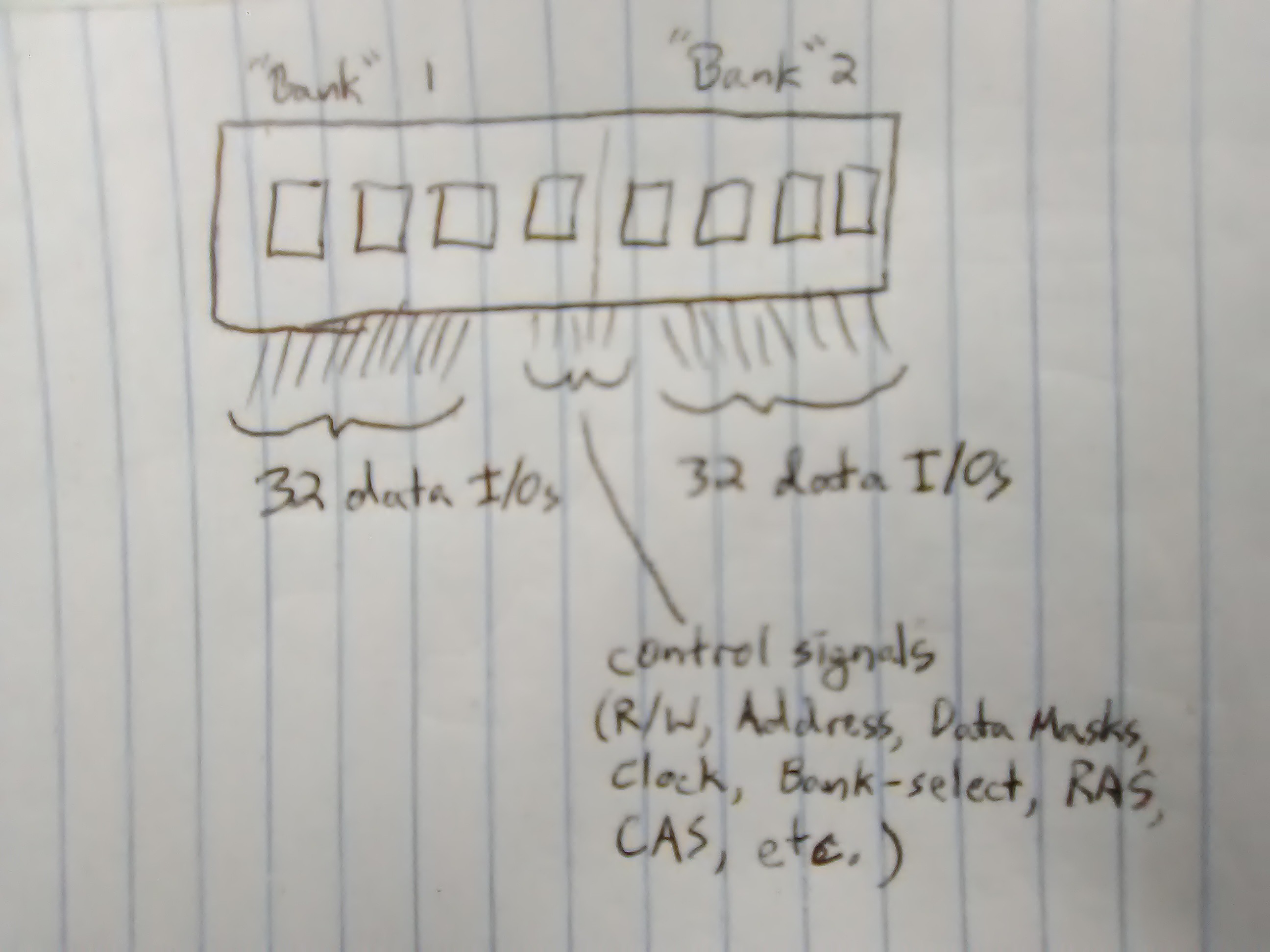
On a PC-100 SDRAM DIMM, there are two separately-controllable "banks" of 32-bit wide memories. It is technically possible [to some extent] to have these two banks running separate read/write operations simultaneously. Thus, it's possible to have one bank, 32bits, reading [outputting data] at the same time the other 32-bit bank is writing [inputting data].
That's a *huge* part of sdramThing. But I'm not going into that, here.
A key factor of #sdramThingZero - 133MS/s 32-bit Logic Analyzer is that I intend to interface all 64bits [and more] to an 8bit bus... and... that 8-bit bus I'd like to be quite simple e.g. not having 8 separate "Byte-Select" signals. Ideally, something similar to a LPT port, or like a character-LCD... 8 data I/O's, Read/Write, strobe, and maybe one or two register-selects... something like that. [For some reason I kinda want this to work with USB-LPT dongles, though it's mostly aimed at single board computers with their own GPIOs].
OK, that's the jist.
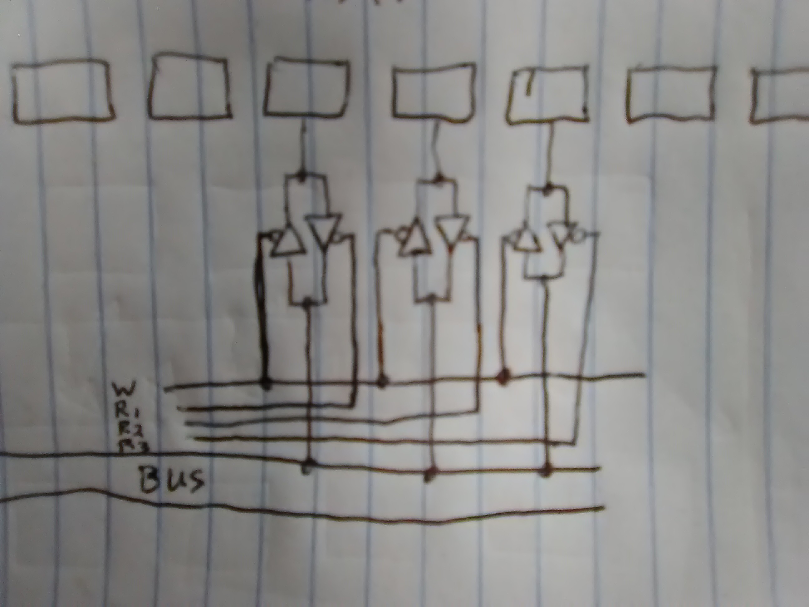
Now, The obvious solution is to just wire 'em all together in 8-bit groups, then use the SDRAM's Data-Mask [DQMB] pins to select which byte to access. Those DQMB pins could be wired to an 8-bit D-latch register like a 74HC574.
BUT: another key factor of this project is that the memory banks are ALSO used *separately* from the data-bus... So, all those data I/O bytes can't be wired directly together...
So, now the next obvious solution is to isolate them from each other and the bus when doing other things, then connect them to the bus when necessary. 64bits is 8 bytes. An e.g. 74HC245 could handle each byte's bus connection, so 8 chips for arbitrating 8 bytes onto the bus. Now, each of those chips has an Output-Enable pin and a Direction pin, so now we need 16 additional control signals on our bus. So, now we need Two 74HC574 8-bit D-Latch registers to set up a read/write on the bus. We'll need two register-select wires to carry the three states [w Direction register, w byte-select register, r/w data byte]. And we'll need glue logic to decypher those two binary signals into three control signals.
We're at 11 chips, now. Just to connect the memory to the bus. [Nevermind all the non-bus-related circuitry!]
So, I'mma step back and think of other options. And I've come up with *numerous*.
-----
Here's the recent thought:
In my case I don't often need to randomly access any byte from the bus; most of the time I'll be reading/writing huge blocks in sequence...
Also, the memory is *huge* [for my needs], we can sacrifice half of 128MB and still be doing great.
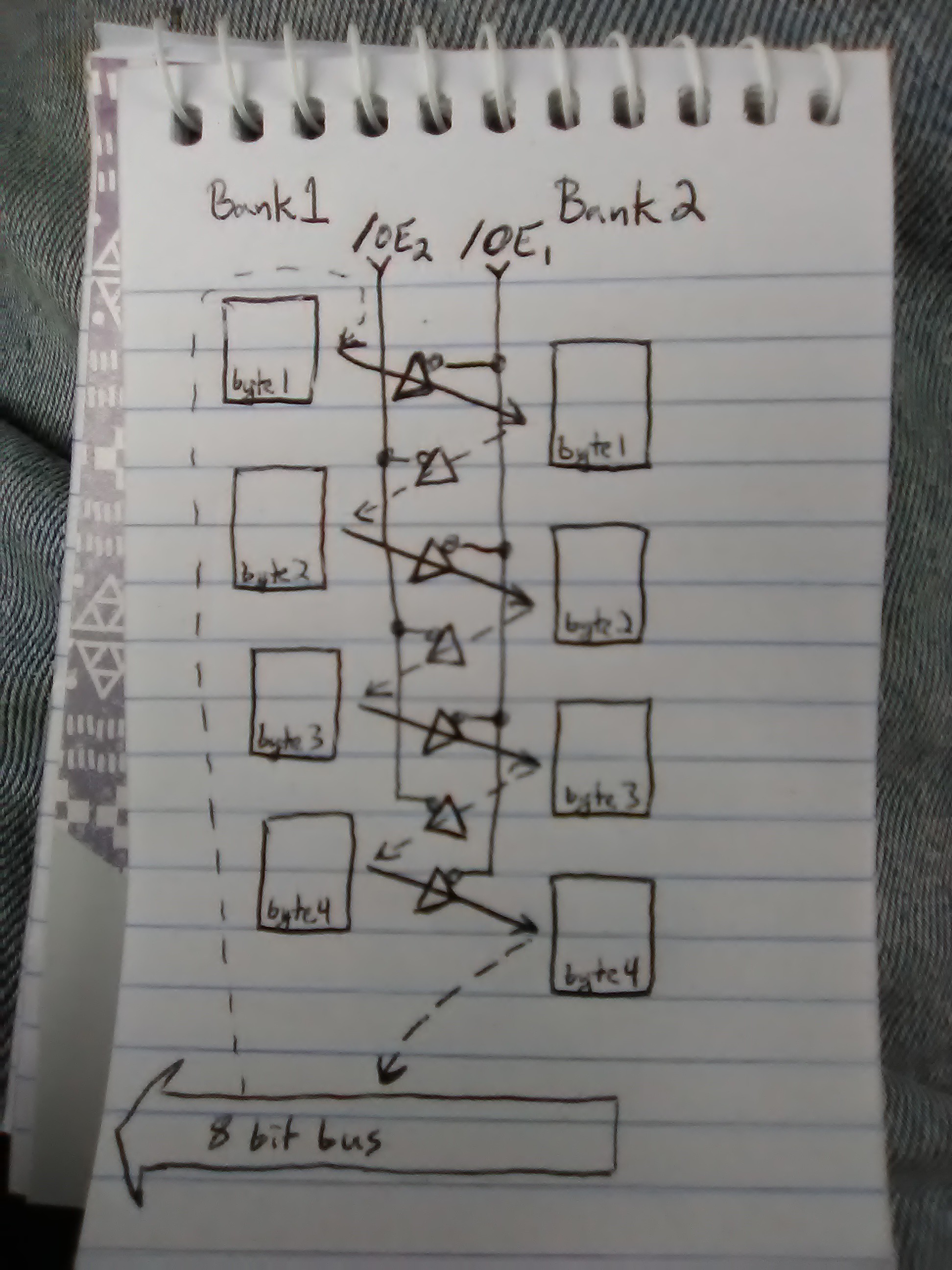
So an option is to use a shifting method; connect the two 32-bit banks together such that e.g. bank1-byte1 is written to bank2-byte1 [and bank1-byte2->bank2-byte2, and so forth], then in the next operation bank2-byte1 [which now contains the data from bank1-byte1] is written to bank1-byte2, and so-forth.
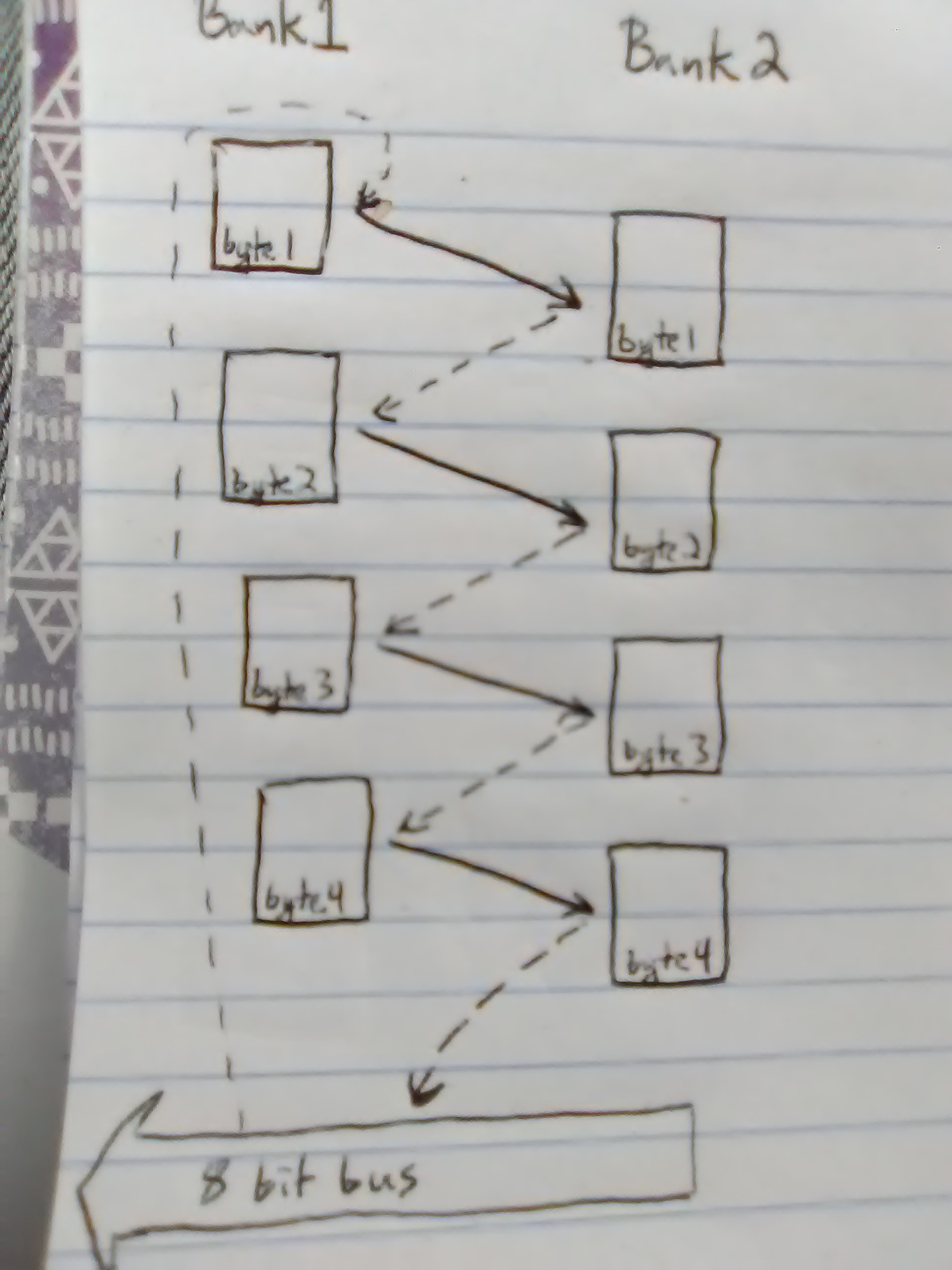
Thus, the data shifts through the bytes, and only one r/w byte needs to be connected to the bus.
Of course, this destroys the data in one bank... but we have PLENTY of RAM, and [I think] can limit the "destruction" to a single page [bytes!], which could simply be a designated "temporary" page...
"But Wait! You can't just wire the bytes like that directly, otherwise there'll be contention, you still need some buffers with output-enables, etc."
True, but, note that now there's only *two* output-enables instead of 8, and no direction signals. Also, we may be able to use the SDRAM's output-enables, etc. so as not to need anything between the bus. And now we're down to seven unidirectional 74HC244's, instead of eight bidirectional 74HC245's.
Now, for some reason I also seem to have a bit of a fixation on trying to limit the active circuitry to that which the SDRAM already has... E.G. those buffers with output-enables seem a bit redundant, seeing as how the SDRAM inputs/outputs already have output-enables, etc. It's *not* redundant, in this case, they serve different functions. But, I still have this strange fixation trying to reduce external circuitry to passive components, letting the DIMM module do everything possible...
So, check this out:
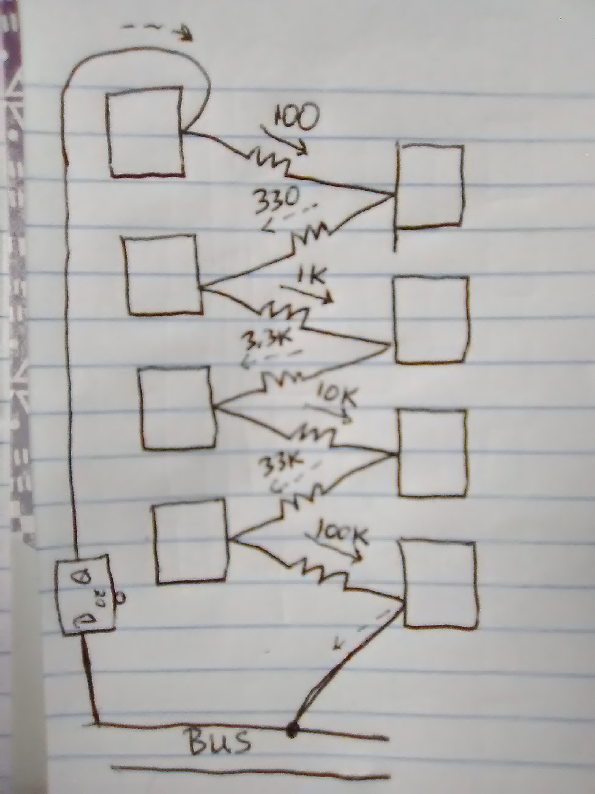
I'm not yet sure about the bus connection, nor how it will interact with my non-bus memory-access circuitry, but it's an interesting concept.
Basically, each input is fed by a voltage divider from two sources, such that 1/4th of the signal comes from the undesired source, while 3/4ths comes from the desired source. I'm pretty sure these are within Vih/Vil specs, thus the little bit of spill-through from the undesired source gets ignored.
This, I think, is right about the limit for such a structure in the CMOS realm... wouldn't feel comfortable with 10ohms [too much load], nor 330K [gotta overcome input capacitance==slower].
Interesting how it just fits.
I've some earlier ramblings on the matter at:
https://hackaday.io/project/10119-sdramthingzero-133mss-32-bit-logic-analyzer/log/159576-todos
And I think I'll stop appending to this log, now, and throw future thoughts in future logs, here.
Discussions
Become a Hackaday.io Member
Create an account to leave a comment. Already have an account? Log In.