How many projects have you done on a protoboard and would like design a pcb? The printed circuit board is the final stage of the project and it is essential for us to test a prototype and launch our products.
However, many people find it difficult in how to design a pcb. In this article, we want to give you 7 tips about how to design a PCB with NEXTPCB Low Cost PCB.
First, we must start with a prototype at Protoboard, after assembling the circuit, perform all possible tests and ensure that it is working as desired. Subsequently, we must move to the stage of design a PCB from the drawing of the electronic schematic.
1 — Designing the Electronic Schematic
The electronic schematic of a project is a fundamental step. In this step, we will design the protoboard electronic scheme in software to design pcb.Among the various software, we recommend using Kicad software. It is free software, has a large community, and has 3D visualization, in order to facilitate the visualization of the final prototype.
Through this software, be aware of the design of your electronic diagram and avoid any error in the phase of drawing the electronic diagram. If an error occurs in this step, it will influence the design of the PCB layout, as the layout depends on the entire electronic diagram design.
In order to avoid errors in the layout, perform the assembly process from the built layout
First, disassemble the entire circuit, use your electronic software diagram and perform the assembly. If the project works, it means that the layout was designed correctly.
In addition, ensure a good organization in the structure of your layout. Always indicate the components with their respective names and values, use observation notes, and organize the regions of the electronic scheme by function blocks.
This will help you understand the functionality of each block and have an overview of your project organization.
Always remember, the organization of the layout of the electronic diagram is fundamental for the stage of design a PCB.
So, one of the things you should consider is to use the grid in your projects.
2 — Use the Grid in your Projects
The grid is a mesh with several divisions that use points or squares. Many beginners do not give importance, but it is crucial in the development of projects because it facilitates the orientation and organization of the electronic components in the diagram design and in the design a PCB project.
Below are two examples of using the grid. First, we have the grid in the drawing of the electronic diagram.

Figure 1 - Grid in Electronic Schematic.
Note that all elements are arranged at an equal distance and fully aligned vertically. This helps in the process of analyzing and visualizing the circuit.
Next, we have the application of the grid in the construction of the design a PCB.
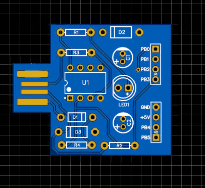
Figure 2 - Grid in PCB Design Layout.
If you analyze the circuit board above, most of the components are aligned and symmetrical, because the grid allows us to organize and align them through the grid.
The result of this process is presented below.
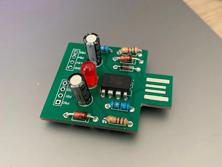
Figure 3 - Result of the PCB Design.
Note that the 2 capacitors and LEDs are aligned and with practically equal distances between them. In addition, the CHIP is aligned with the LED and the resistor groups are in symmetrical regions.
Finally, we have a USB connection. Note that it is centralized with the electronic board structure.
Therefore, the grid is an organization tool, which was born with the aim of facilitating your organization and improving the quality of the design a pcb.
3 — Calculate the track width of the design a PCB
The tracks are like wires. They are the elements that allow the electric current to flow in your electronic circuit. As we know, the higher the value of the electric current, the larger the section of a conductor must be, so that it can allow the conduction of current.
In the design a PCB, it works with the same principle and therefore, we must perform the proper calculation of the width of the tracks.
For this, we will use software that helps in the process of dimensioning the trails.
You can access the link on the Digikey website and enter the current and temperature parameters for the project. Later, the website will inform the ideal value of the width of your trail. It is important to highlight that the site is safe and uses the equations of the IPC-2221 standard to calculate the width of the tracks: Access the link and calculate the track width
When you access the website, it will appear in the following window presented below.

Figure 4 - Trace Width calculation.
For this calculation, you must enter the current value of the track, the thickness of the copper, the temperatures, and finally, the length of the track. This latter information can be obtained from the track information within the project software environment.
From this, the software will inform two types of widths: for internal tracks (multilayer) and external tracks (single and double layer, as shown below).

Figure 5 - Result of Trace Width.
In addition, you will know the resistance, voltage drop, and power losses along the trail.
Therefore, from this application, you will be able to determine the width and other properties of your project’s tracks with good security.
4 — Auto Router and Auto Placement in the design of a PCB
These are two tools that are widely used by many beginners: the auto-router and the auto-placement. However, be very careful. It is not very ideal to use them in your projects.
Auto-routing is a process in which the software routes all tracks for you.
Several softwares have the Auto router, however, in the process of use, we noticed a big mess on the tracks, when this tool is applied. Although the software has an excellent trail routing system, we realized that it is risky to use it for this.
In addition to being risky, many designers do not recommend and do not use it, as the software itself does not understand the characteristics of operation, signal levels, specification of electronic components, and other characteristics that affect the organization of the trails.
As we know, certain trails that pass certain signals cannot be close and need to be built with great care. Therefore, we suggest that you always do the manual routing process. This helps to avoid errors, interference, and helps to improve the design of a PCB.
Through the manual process, we were able to analyze the structure of each trail, perform individual routing based on its signals, and ensure better organization and safety in the structure of our project’s trails.
In addition to the auto-router, many use auto-placement. This feature is another problem that can occur in your PCB projects. It is not recommended to use it, because once again we quote: the placement has the purpose of organizing its components automatically and this can cause major problems.
When you use this feature, some components can suffer major problems, as some, for example, dissipate a lot of heat, and others are sensitive to heat.
Analyzing these components, the placement does not understand and can leave them close to each other and, consequently, generate damage to the sensitive components of the circuit. As well as, generate other design problems.
Therefore, avoid using auto-placement and auto-router. Always prioritize carrying out your work manually and you will have the greatest possible control of the electronic components and the tracks of your PCB projects.
5 — Heat Dissipation on the PCB design
Several electronic components dissipate a lot of heat when they are in operation in the circuits. Among these devices, we highlight voltage regulators, resistors, and drive drivers, for example.
To avoid this problem, we can use rectangular copper regions under the IC that dissipate a high-temperature value. In this way, you reduce the temperature and guarantee the life of the CI. This is shown in the figure below.

Figure 6 - Example of cooper-filled region.
As you can see, inside the Ci there is a red rectangle. This rectangle is a copper-filled region and can assist in dissipating heat from your IC.In addition, I have never left devices that dissipate large amounts of heat that should not be placed in the same region. Keep them as far away as possible.
Devices that are more sensitive to temperature should be away from high-temperature devices, so you should place them in cooler regions of your printed circuit board to ensure good security in your printed circuit board design.
Print information on the Silkscreen layer of your PCB
The silkscreen layer is intended to print information and also your company logo. It is a layer that aims to print information on the bottom and top surfaces of your PCB design.
Thus, the silkscreen layer has some objectives such as:- Information of connections and elements of your board;- Assist in the manual assembly and maintenance process;- Aesthetics and design.
See, for example, the sign shown below.

Figure 7 - Example of silkscreen in PCB Design.
As you can see, there is a layer of texts, symbols, and images on the blue-colored region of this electronic board. All of these elements are printed on the silkscreen layer.
All of these texts will assist in the welding of components, as they all carry the name of the element (R1, R2, C1, U1) that must be welded in a certain position on your printed circuit board. In addition, it helps in the maintenance process, because in the future, a new user can access this information on the PCB and obtain the value of each component through the information of the silkscreen layer.
Therefore, always try to use the silkscreen layer. It will help you in the process of organizing your project information and in the assembly process.
Build your first prototypes for your projects
Develop the first prototypes of your printed circuit board. Many people believe that developing a printed circuit board is a high-value service, but with the services of manufacturing companies, you can produce your first 10 boards for $ 5.
These are low-cost boards that allow you to evaluate the performance of your prototype.
In addition, there is a company like NEXTPCB, which helps you in the process of developing your board and offers you can test to create your first boards.
To perform this process, you need to enter the website, upload the Gerber files.