 oneohm
This Log entry addresses the readiness for manufacturing and the path from prototyping to production for each component of the BYTE.
Many of the parts for prototyping have been produced either with a 3D printer or a fiber laser engraver. These tools are excellent for rapid design iteration, but are not ideal for production quantities.
Purchased Parts:
The silicone enclosure, M2 screw, o-ring, and flat CAT6 cable are commercially available purchased parts.
Plastic:
Plastic parts are 3D printed for the prototypes, but would transition to injection molding for production. They have been designed in a way to simplify the injection molding tooling and thus minimize the cost. Currently the stem portion is printed as three pieces, but when molded, can be combined into a single part.
Since the plastic parts are approximately the same size and volume, they can likely be molded simultaneously in a family tool, further reducing cost.
Silicone Disc:
Using sharpened pieces of tubing, I am punching this part from 0.032" silicone rubber sheet for the prototypes. This process is really tedious, but fortunately these parts can be rapidly made a whole sheet at a time with a steel-rule die and a press. There are also many companies that specialize in producing this type of part.
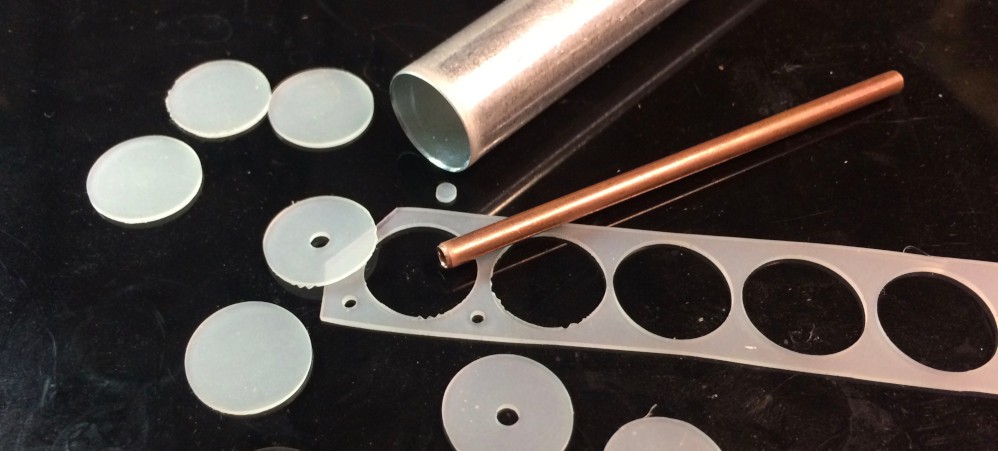
Common Contact:
I am currently laser cutting this part from 0.1mm copper sheet; this process is quick and easy and scalable up to small scale production quantities. Larger scale production would be better suited to photo-chemical etching, where large sheets containing hundreds of parts can efficiently be produced.
Force Sensitive Resistor Disc:
These are individually laser cut from 3M 1706 conductive sheeting. Larger quantities would be die cut with a steel rule die, possibly with the same tooling (or even at the same time) as the silicone disc.
Stem Force Sensitive Resistor:
This part is produced from the same 3M conductive sheet backed with 3M 468MP adhesive transfer tape. This is currently done by laser cutting the conductive sheet, then applying them to the transfer tape and manually cutting the profile. This is done because the laser is able to cut the conductive sheet due to its dark color and high carbon content, while the transfer tape is basically invisible at the wavelength of my fiber laser, rendering it uncuttable.
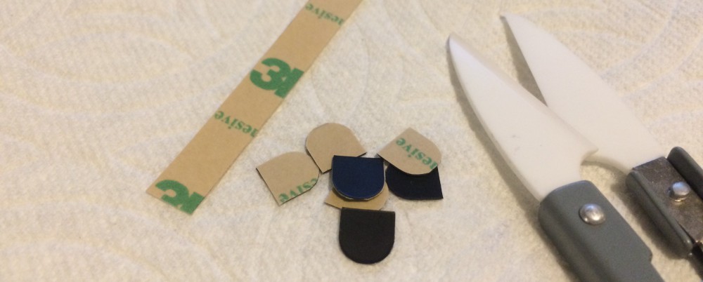
Production quantities would be produced by laminating the conductive sheet to the transfer tape, then using a steel rule die to kiss-cut the parts. This leaves the transfer tape backing intact, but cleanly cuts through the conductive and adhesive layers, leaving an easily manageable sheet of stickers ready to apply.
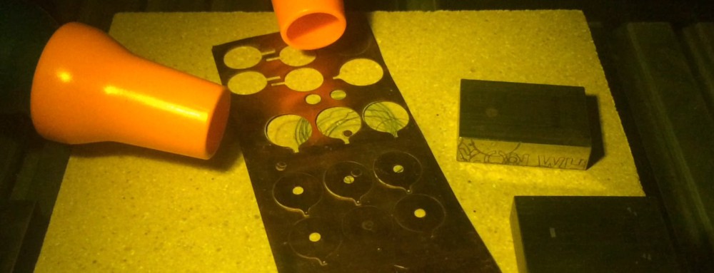
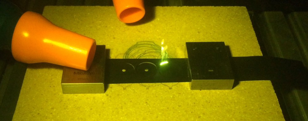
PCBs:
My prototype process for PCBs is to first isolate the tracks by laser ablating the copper. UV curing soldermask resin is then applied over the whole thing and--once cured--the laser is used again to selectively remove the soldermask exposing the required pads. After cleaning up the residue with Isopropyl alcohol, I hand drill the holes on a drill press. Next they are dipped into MG Chemicals 421A Liquid Tin to improve solderability and prevent oxidation. Finally I cut the board outline on a mini tablesaw, and finalize the shape with a bench grinder.
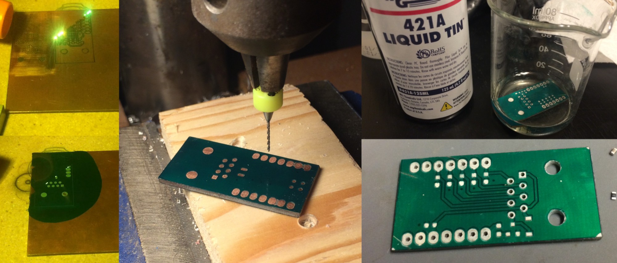
The convenience of quickly producing my own circuit boards is great for prototyping, but for larger quantities a traditional PCB fabricator is the way to go. In the last few years the cost and lead-time for commercially produced PCBs has become very reasonable.
For these small boards, it makes the most sense to create an array of arrays. The three boards required for each BYTE (Nav, Bite, and Control boards) will be arranged into a rectangular board, which will in turn be tiled into a more manageable size with perhaps 10 or 20 complete sets per panel.
Discussions
Become a Hackaday.io Member
Create an account to leave a comment. Already have an account? Log In.