 Tijl Schepens
As almost every Electronics project, it starts with designing the hardware. I've kept the schematic entry as
simple as possible. Copying the largest part from the typical application diagram in the datasheet.
Some parts still have to be dimensioned:
- Fanin resistor. This resistor determines the maximum amount of current the device is allowed to pull from the KNX bus. KNX is very strict the amount of current that can be consumed and at what rate. They specify that you should select a Fanin which matches closely with the current consumption of your application.
Even though I'm not planning to power any peripherals, I've selected the maximum current setting of 40 mA just in case ;-) - Vfilt buffer capacitor. This buffer capacitor is essential in a KNX system. It is used to handle load changes. When for example and LED is switched on, the device current consumption increases instantly. However the KNX standard forbids that the current at the bus side changes instantly. So the buffer cap must deliver the instantaneous current. Then the transceiver is responsible for recharching the capacitor at a fixed current rate. The current slope on the bus is dependant on the Fanin setting selected with the Fanin resistor.
Another task of this capacitor is keeping the MCU alive long enough when the bus power goes away. This is necessary as the MCU must be able to write away essential data to non-volatile memory when the bus power drops.
In this situation the Raspberry Pi is powered independent from the KNX bus and thus not data needs to be saved. The only requirement is that load changes need to be handled well. As there a no peripherals introducing load steps, I selected a low capacitor value (47 uF) in order to keep it small. It is possible to use an even smaller one, but I wanted some margin just in case I want to power external circuitry in the future. - DC-DC converter inductors. The transceiver has two DC-DC converters. One converter always generates 3.3 V and is also used to power the transceiver itself. The other one can be set to a voltage between 1.2 V to 21 V. Both are capable of delivering 100 mA (if the input power allows for this of course). It is however not possible to use both to deliver 100 mA at the same time as the KNX bus cannot deliver this amount of power.
For the second DC-DC converter I've chosen 9 V. This allows to power for example and Arduino in the future.
To select the right inductor, I've used RedExpert from Wurth Elektronik. A very simple and useful tool to select the right inductor for a variety of converters. Here you can find the design. I've selected 744043221 as it has lower total losses and is almost the same size as 744042221 (just a little bit higher). - ADC: The NCN5130 has an ANAOUT pin which outputs some diagnostic information. On this pin there is an analog voltage which represents a system parameter. For example the bus voltage or current can be monitored this way. Through UART it can be changed what is monitored through the pin.
Honestly I've been lazy here. I've just selected an ADC which was in the KiCAD libraries. As I was not really that interested in the diagnostic output, the accuracy did not really matter for me.
I've settled with the ADC081C021CIMM from Texas Instruments. It's a simple I2C ADC.
The Raspberry Pi is not being fed from the KNX bus as there is not enough available power. As the device must be able to operate even at bus voltages as low as 21 V, the maximum available bus power is 21 V x 40 mA = 840 mW. And that is assuming that the NCN5130 is 100% efficient which is not the case...
To calculate the most important component values, there is a handy calcualtor sheet.
After some weeks of work, this is the outcome:
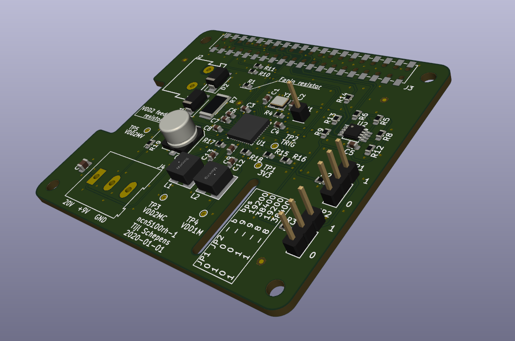 The two feedback resistors for the second DC-DC converter were placed at the left of the PCB far apart so that they would be easily accessible for resoldering. This way the output voltage can be adjusted easily.
On the right hand side of the PCB there are two 3-pins headers which can be used to select the UART baud rate and the usage of a parity bit.
Discussions
Become a Hackaday.io Member
Create an account to leave a comment. Already have an account? Log In.