 Leonardo Ward
Similar to our previous post that discusses our plans for the Buoy, there is also a plan for the Onboard Gateway. The following image presents the Hardware Block Diagram of the Onboard Gateway V1.0 (our previous design). The different colors are used to group different elements on the design, and facilitate the comparison between different diagrams. The numbers near the peripherals in the microcontroller represent the amount that is being used.
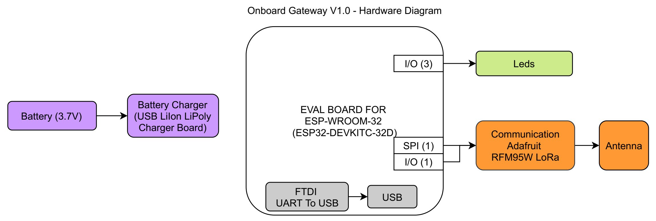
Design elements:
- Microcontroller (ESP32)
- LoRa Transceiver
- Battery Charger
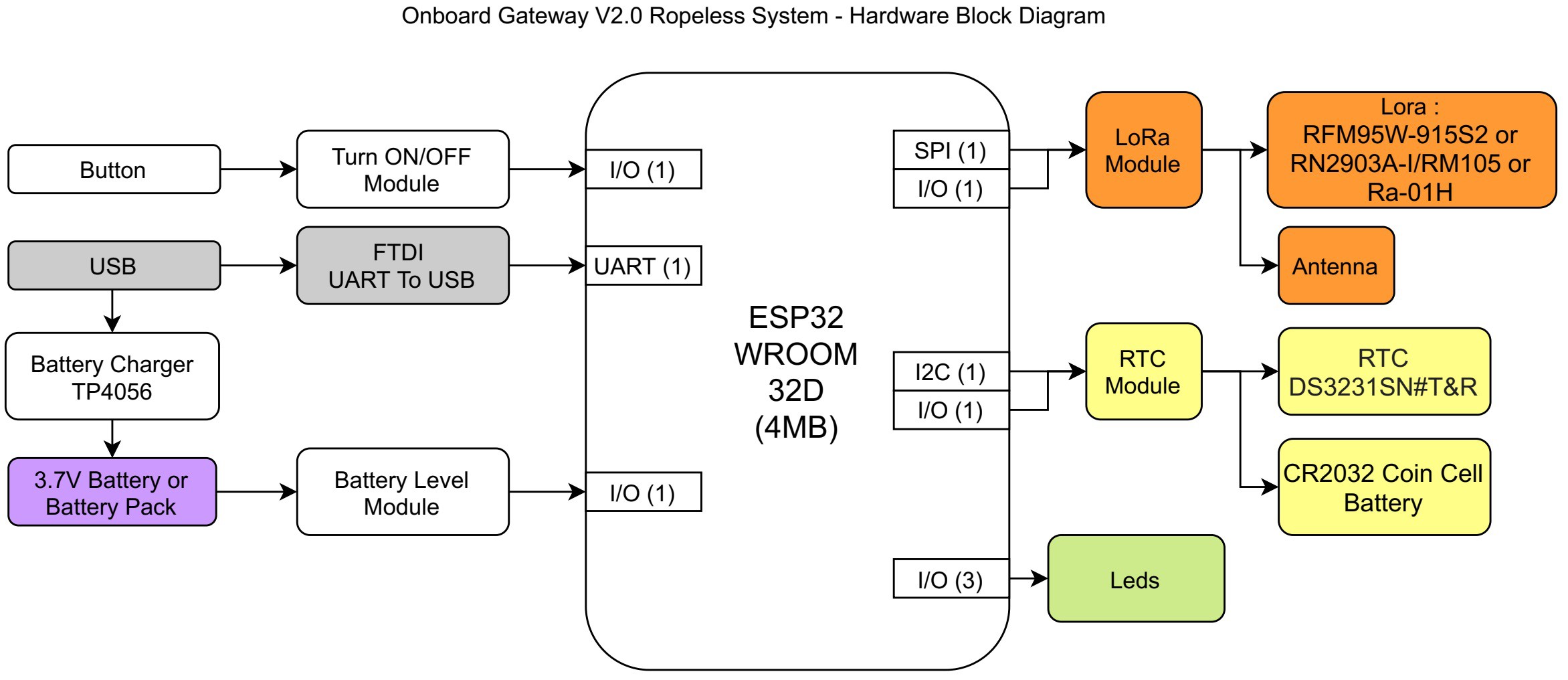
The previous design used different self-contained development boards to reduce the development time. For the new version we will replace the development boards with the main components in them and place the adapting circuit in our own PCB. Usually a change like the one mentioned reduces the overall price, but not always, it is always important to have the reference price of the development board.
The following image contains the Hardware Diagram for the new Onboard Gateway v2.0, it contains mostly the same basic elements (and therefore features).The most important added feature in the new design is the real time clock (RTC).
Discussions
Become a Hackaday.io Member
Create an account to leave a comment. Already have an account? Log In.