For my Native Instruments KORE 2 BLE MIDI conversion project I needed a new display that would mechanically fit into the display frame of the old display. After searching for a long time I finally found a suitable OLED display from Microtips/Raystar called REX012864GWPP3N00000
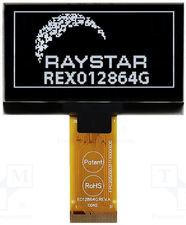
This is a white OLED display with an SSD1309 controller. Compared to the more popular SSD1306 which has a built-in charge pump the SSD1309 requires an external high voltage (12-13V) input. As I was not able to find any suitable breakout boards for this OLED display I made my own. And this also allowed me to make it in a form factor that fits well in the KORE 2 encapsulation.
I ran into several problems, amongst others that the datasheet on Mouser’s website had the totally wrong pinout for this display. And the datasheet also had very limited information about how to get it connected. But after a lot of studying I was finally able to pull the complete circuit together.
12/13V boost circuit
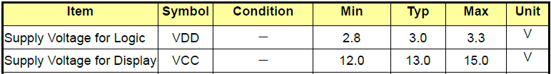
As the SSD1309 does not have an on-board charge pump I had to make a boost circuit. The datasheet specifies min12V max 15V (typ 13V) for the Display supply voltage, so I chose the MAX607 Step-Up DC-DC Converter device for this design which can boost an incoming 3-5V to desired level. The MAX607 datasheet specify 12.5V as the maximum output voltage, but the Absolute maximum ratings have a limit of 15V and the electrical characteristics use VOUT=13V as condition for many of the parameters, so it should be OK to run the MAX607 with a 13V output.
As I have seen other OLEDs require different display voltages I made the design with an optional configurable output voltage different from 12V.
Although the logic for the OLED display needs 3V (max 3.3V) I chose to run the boost from 5V as it can be taken directly from the USB connector in my KORE 2 controller rebuild project, and the 3V is through a regulator with limited output current.
The circuit is taken from the MAX607 datasheet reference schematic, and my component selection leaves options for 12V and 13V output. Other voltages from 5V to 13V can be configured by changing R4 and R5 values according to formula VOUT = 2R4R5+1
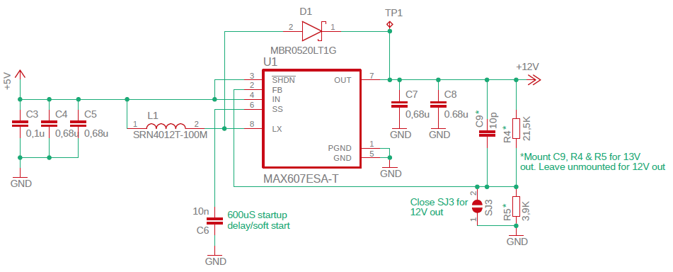
For 12V C9,R4 and R5 should not be mounted, and solder jumper SJ3 should be closed.
For 13V, keep SJ3 open and mount C9,R4 and R5.
OLED interface
For the OLED interface I designed it configurable for I2C or SPI connection. Notice that although the OLED display datasheet refer to 3-wire SPI mode e.g. for the D/C# signal description, there is no option for 3-wire SPI operation as the SSD1309’s BS0 signal is internally tied to GND. Only 4-wire mode is possible for the SPI option.
R1 must be set according to the OLED driving voltage to give an IREF current of 10uA: R=OLED driving voltage- VCC10A
R2 is a pullup for the reset pin in case it is left unconnected.
R3 is an optional pull down for the CS# line. It should strictly speaking not be needed, as in 4-wire SPI mode this line is actively used by the display interface, and for I2C mode it looks from the datasheet like this line is internally tied to ground. But as this line is not used for I2C mode, and the display will not function if CS# is not pulled low I added this as a precaution.
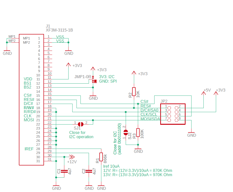
SPI operation
For SPI operation solder jumper JMP1 should be closed towards ground. The other solder jumpers should be kept open.
I2C operation
For I2C mode the SSD1309 controller uses two pins for data D1 and D2, and therefore SJ1 must be closed to connect these two pins. SJ2 is connected to SA0 (Slave address bit 0) to configure the I2C address. With SJ2 closed to ground, the I2C slave address is 0b0111100 (0x3C). If SJ2 is left open the SA0 line must be driven from the interface. Driving it high will set the slave address to 0b0111100 (0x3D).
PCB layout
The PCB is made using 1mm FR4 laminate and with a shape where it can be easily fitted inside the back of the KORE 2 housing.
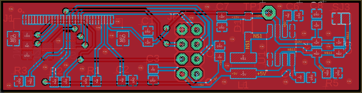
I ordered my PCBs from JLCPCB, and must say I am very happy with both the ease of ordering, the price, speed of processing/shipping and the quality of the board. They are definitely my go-to PCB manufacturer from now on.

Completed PCB. The silk screen had some conflict with the pads, but this has been corrected in the latest silkscreen gerber file. Solder jumper SJ3 closed and R4, R5 and C9 not mounted for 12V operation.

Solder jumper JMP1 closed towards ground to enable 4-wire SPI mode. The other solder jumpers are for I2C mode.
Testing
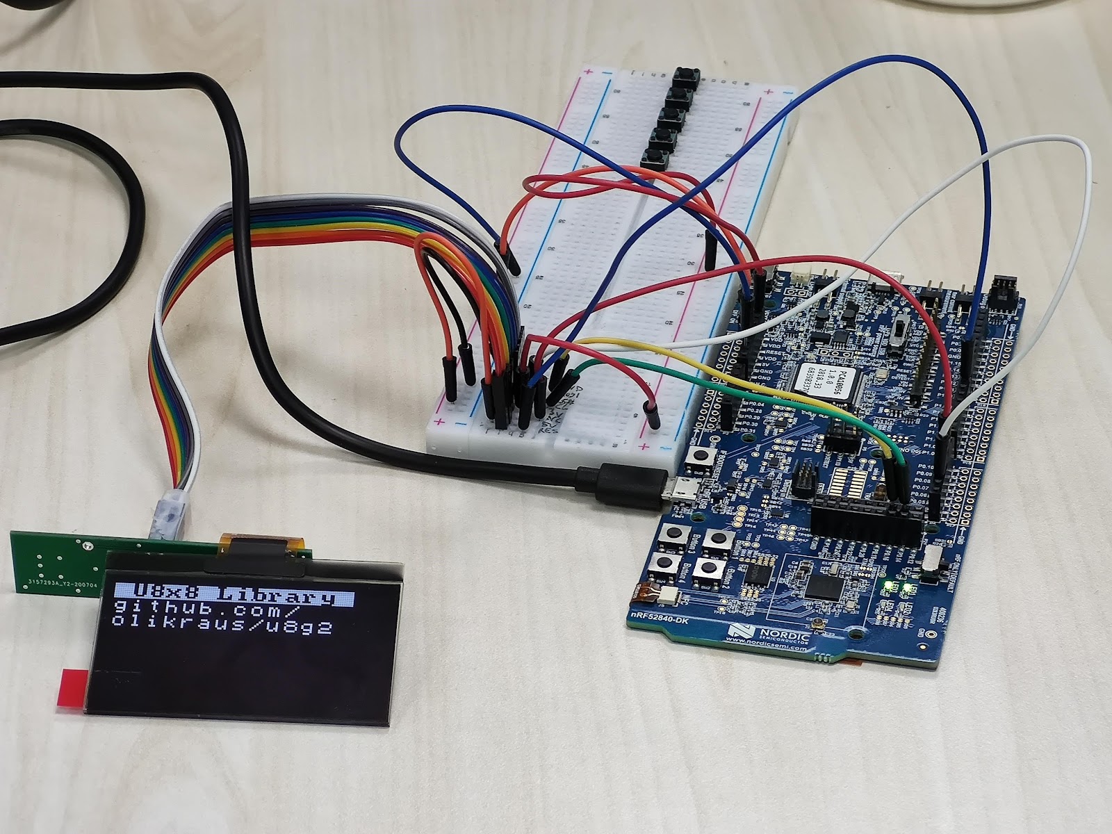
To test the board I connected it to an nRF52840-DK programmed with an Adafruit Arduino bootloader (https://hackaday.io/project/171550-ble-midi-controller-conversion-of-ni-kore/log/177876-getting-ble-midi-running), chose the “Adafruit itsybitsy nRF52840 express board” in the Arduino IDE, installed the u8g2 graphics library and ran the u8x8 Graphics test example.
Connections:
OLED breakout | nRF52840-DK | Itsybitsy nRF52840 |
1 (RES#) | P1.08 | 7 |
2 (+5V) | +5V | USB |
3 (D/C#) | P0.07 | 9 |
4 (+3V3) | VCC | 3V |
5 (CLK) | P0.13 | SCK |
6 (CS#) | P0.05 | 10 |
7 (MOSI) | P0.15 | MO |
8 (GND) | GND | GND |
The display constructor setup in the u8x8 library should be set up as follows:
//U8X8_SSD1309_128X64_NONAME0_4W_HW_SPI u8x8(cs ,dc ,reset);

U8X8_SSD1309_128X64_NONAME0_4W_HW_SPI u8x8(10, 9, 7);
And as the display will be mounted upside down the setup function need to include
setFlipMode(1):
void setup(void)
{
  u8x8.begin();
  u8x8.setFlipMode(1);  //Flip display
}
I have attached the modified GraphicsTest.ino file to this project.
Picture below shows the test setup running the u8x8 graphics test from the u8g2 library.