 Charlie Smith
Because this project has been going for a while (started about 20 months ago as of writing this), I will make a summary of the progress made up to to when I created the project here.
The general idea of the computer is the same as the one designed by Ben Eater. However, I want to make a computer which firstly I have designed, and secondly is capable of running something interesting. As such, the general design will be the same. However, the computer will be 16-bit and have some redesigned modules.
Before this project I had done some electronics projects, but basically only for GSCE electronic at school. This was my first large scale unguided project, and also my first with properly build PCBs. So take that as a warning that there are going to be some stupid choices made in the design.
DESIGN
Firstly, I needed to pick the modules to include in the initial design of the computer (with the idea that mode would be added later). Clearly there are some that are required for the computer to function which I will call core modules while others add additional abilities to the computer which I will call function modules. Also all modules should have LEDs to display the value currently stored in the module.
CORE:
- Clock
- Synchronizes the computer so everything will work correctly
- Program counter (PC)
- Stores the memory address of the next instruction to read
- Memory Address Register (MAR)
- Stores the memory address which the RAM either read or write to
- Random Access Memory (RAM)
- Stores all the working data and instructions (instructions could be read from some other memory)
- Current Instruction Register (IR)
- Stores the data for the current instruction being run
- Made of an 6-bit OPCODE and OPERAND
- To allow access to all of RAM, this needs 6 bits for the OPCODE and 16-bits for the OPERAND. As such this can be a 2 word register.
- With 26 bits for the OPERAND we can have several modes of outputting the OPERAND to the bus
- FAST: 10-bit OPERAND so only the first word needs data make the operation faster to execute
- FULL: 16-bit OPERAND so all of memory is accessible, but both words need data
- MLT_0: First of two 13-bit OPERANDS allowing for two arguments to an instruction
- MIL_1: Second of two 13-bit OPERANDS allowing for two arguments to an instruction
- Control Logic
- Decodes the OPCODE and any flags to a control word used to control all parts of the computer
FUNCTION:
- Arithmetic Logic Unit (ALU)
- Performs all mathematical and logical operations using values in the A and B register
- Initially this is limited to addition and subtraction
- A Register
- Stores the value currently being worked on by the ALU
- B Register
- Stores a modifier value which the ALU uses to act on register A
- X Register
- Index register, used to store a pointer to a value in an array
- Needs to be able to increment by 1 without using the ALU
- Output Register
- Stores a value to be displayed in some way
- Should also have a decimal decoder of the value stored
- Input Register
- Used to store a user input
- Program Memory Address Register (PMAR)
- Stores an address in program memory for an instruction or constant to fetch
- Program Memory
- EEPROM storage of write only data to store instructions and constant for a program
- The actual storage should be easily removable such that the program being run can be changed easily
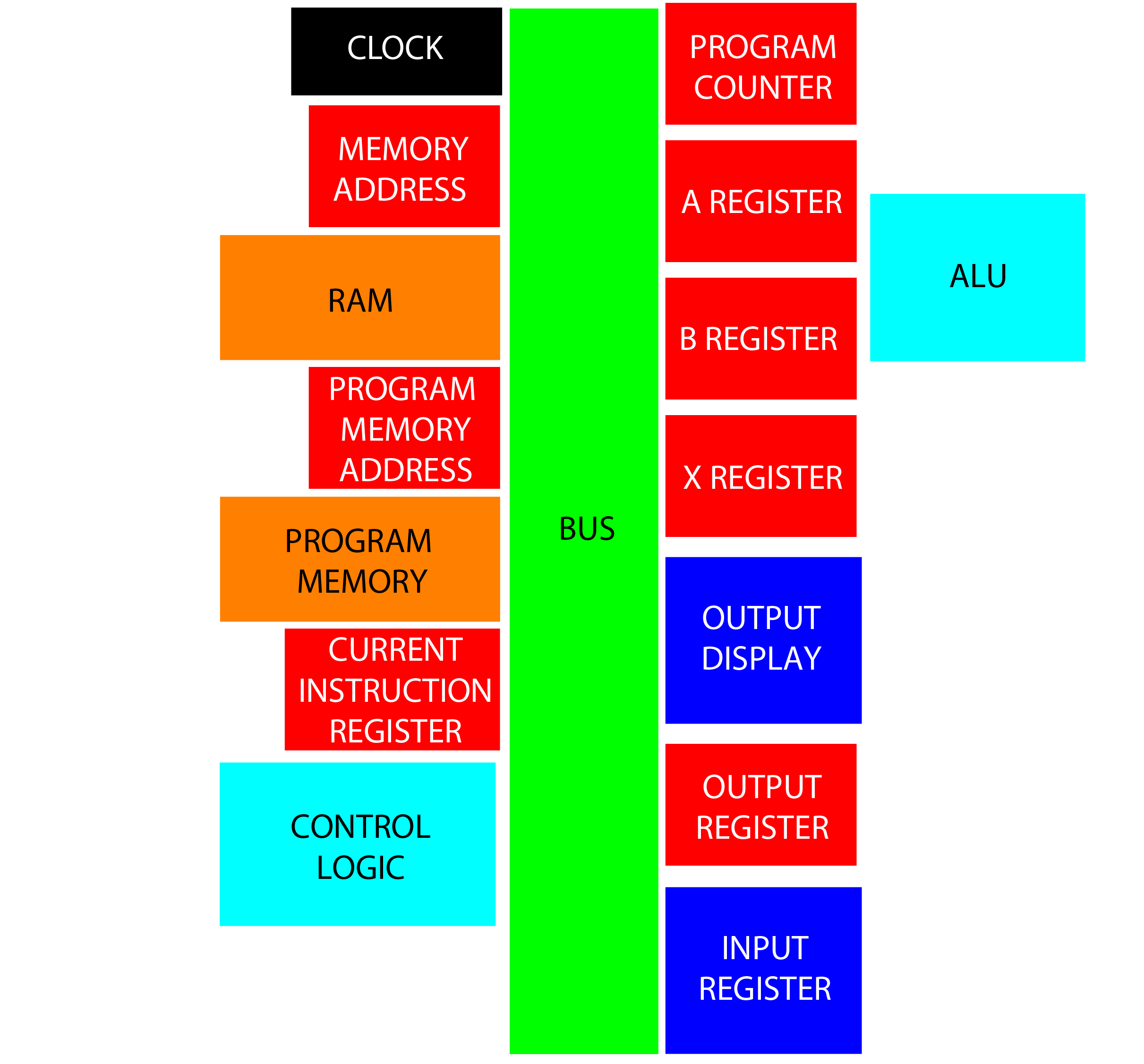
While I could go into the design of each of these modules, this would end up being rather long. So I will summarize the main parts. Firstly a number of the modules are functionally identical, so can use the same base module, possibly with some small changes. So the A and B registers use the same hardware, while the output register is also the same, but does not need the components to output to the bus to be populated. Similarly PC and X have the same hardware, as do MAR and PMAR. The IR can also use the same parts as MAR, but will need to modules to get a 32-bit word, and also need a module to allow for each output mode to the bus. Here are a rough design to the main modules.
Clock:
This uses a CD4047BC low power multivibrator. This uses only a single resitor and single capacitor to control the frequency. As such, it is simple to produce a 50% duty cycle square wave at a large range of frequencies (unlike on a 555 timer). As such, some dip switches can be used to change which resistor and which capacitor are being used, along with a variable resitor for finer tuning of the frequency. The rest of the module is roughly the same as the Ben Eater clock.
Simple Register:
Uses two 74LS273 octal flip-flops to store data, needing an extra 74LS08 AND gate to combine the read data and clock signal. Also uses two 74LS245 octal bus transceivers to output data to the bus. This allows for the module to output the data stored in the flip-flops to be displayed with LEDs, while also allowing for conditional output to the bus. This output method is common to all devices capable of driving a value onto the bus.
Index Register:
Uses the same output method as the simple register, but has four 74LS161 4-bit counters to store the data and allow for the current value to be incremented by one.
Address Input:
This is the data storage part of the simple register, but with no bus output. Instead there is a 16-bit connector for sending the data to some other module.
ALU:
This is rather complicated module, even for just addition and subtraction (which is why no other operations are available), using 14 total ICs. The main ones being four 74LS283 4-bit full adders to perform the operation as well as the same ICs as the simple register to output to the bus. The module also needs to produce signals for when the operation resulted in zero or when the carry bit of the final adder is set. This means that two 74LS02 NOR gates and two 74LS08 AND gates are needed to check if any bit is non zero. There also needs to be four 74LS86 XOR gates for conditional inverting of the B register for subtraction.
RAM:
Yet another complicated module. For the actual storage I am using a pair of AS6C1008 128k x 8-bit low power CMOS SRAM. This particular chip is compatible with the TTL logic of the 74LSxx series chips used everywhere else. However, they use the same pins for data input and output, and so while the same ICs are used as before for the output, they need additional controls for which data is allowed to pass in. I also decided to over complicate things by having a built in read only memory (ROM) to store so initial program to run. The idea with this was to have a some instructions to copy the program from the program memory to RAM, before running the program exclusively from RAM. While this will work, my more recent dealings with microprocessors has made me realize that it might just be easier to only allow instructions to be stored in program memory, and they are copied from there to the IR rather than needing to have all the instructions copied to RAM before the program can execute. However, the design has the ROM, which then needs control over when to output a value from ROM, rather than RAM. For this I am allowing either 16 or 32 words of ROM (4 or 5 bits). This means that if all higher bits are zero, then ROM is enabled rather than RAM. This makes use of a rather complicated layout of two 74LS02 NOR gates, two 74LS08 AND gates and a 74LS04 NOT gate. The clock signal is also decoupled from the rest of the computer using a serial pair of NOT gates followed by a edge trigger using a 1k resister and 10nF capacitor, which I found an explanation for here. The ROM chips don't need to be very large, and because I have already made use of them I am using the same AT28C16 2k x 8bit parallel EEPROMs used by Ben Eater for the original computer.
Program Memory:
This is mostly just the output from the simple register, with an address input. There is also a connector to an external storage cartridge. This and connections for 16-bit address, 16-bit data, power, read enabled and write enabled. The write enabled is available to make programming the cartridge easier, as the EEPROM chips do not need to be removed. For the choice of EEPROM, the AT28C16 used in the RAM do not have enough address bits for the full 16-bit address. While these aren't really needed, the address is available so I am using two GLS29EE010 128k x 8-bit page write EEPROMs. These have more than enough address bits, but unfortunately are a bit of a pain to program (I wont go into it know, but I might at a log about it at some point).
Output decimal decode:
This takes the value in the output register and uses two more GLS29EE010 EEPROMS with a 555 and 74LS76 dual JK flip-flop to scan over each of five 7-segment displays at a high enough rate that they all appear to be on. There is also a sixth 7-segment display that can display a negative sign if the most significant bit is set. This allows for a twos compliment signed value to be displayed. Unfortunately the EEPROMs don't have enough address lines for both signed and unsigned decoding to be stored, so they need to be reprogrammed to changed output mode (rather than just moving the jumper).
Input:
This is just the output part of a simple register, with connection to some external module to actually handle the user input. This other module can be changed depending on the what sort of input is required. This module also need to be given an indication that the control logic is requesting an input (and so the computer is halted), as well as a return signal for when an input is available (so the computer can resume).
Control Logic:
There are two main sections to this module. Firstly there is a micro-instruction register and flag register, made from a 74LS161 4-bit counter and 74LS173 4-bit register respectively. There is also a 74LS02 NOR gate to manage resetting the micro-instruction register and full system reset. The second part to the module is a series of control bytes. These are able to be chained together to form an arbitrarily long control word. Each of these bytes uses a GLS29EE010 EEPROM with an address of the OPCODE from the IR, current micro-instruction and the 4-bits from the flags register. As some of the control bits are active low, there also needs to be a 74LS04 hex inverter allowing for 6 of 8 bits of each control byte to be inverted if needed. This does mean that some thought needs to be given to the ordering of control bits, but most control bits are active high, so there is no point in adding and extra inverter for the final two bits.
That still took quite a while to explain, and doesn't cover all of the computer but hopefully it gives a rough idea of the parts of each module. The next part was PCB design. I will skip over this completely as it was done quite a while ago and wasn't done particularly well.
The next log will go over the build process so far, to catch up to where the project is as of the project being added to hackaday.io.
Discussions
Become a Hackaday.io Member
Create an account to leave a comment. Already have an account? Log In.