 techav
It Lives!
A good first step when starting a new homebrew computer is always the free run test — wire a simple repeatable instruction to the data bus (e.g. NOP), place pull resistors on all CPU inputs, and give it a good clock signal. The CPU will start fetching instructions, incrementing its address bus for every instruction fetch. Since the data bus is hard wired to a single instruction, the CPU's Program Counter register will never branch, just increment through the CPU's address space. This makes a successful free run easy to identify — watch the address bus for an incrementing binary pattern.
My Approach
For an 8-bit microprocessor like the Z80, free run is a simple task. Plug the CPU into a solderless breadboard, ground the data bus, and throw a pull-up resistor on all of its input signals. The Pentium's 273-lead PGA package is quite a bit more challenging to work with — the trusty solderless breadboard just isn't going to work here, and there are many more control signals to consider.
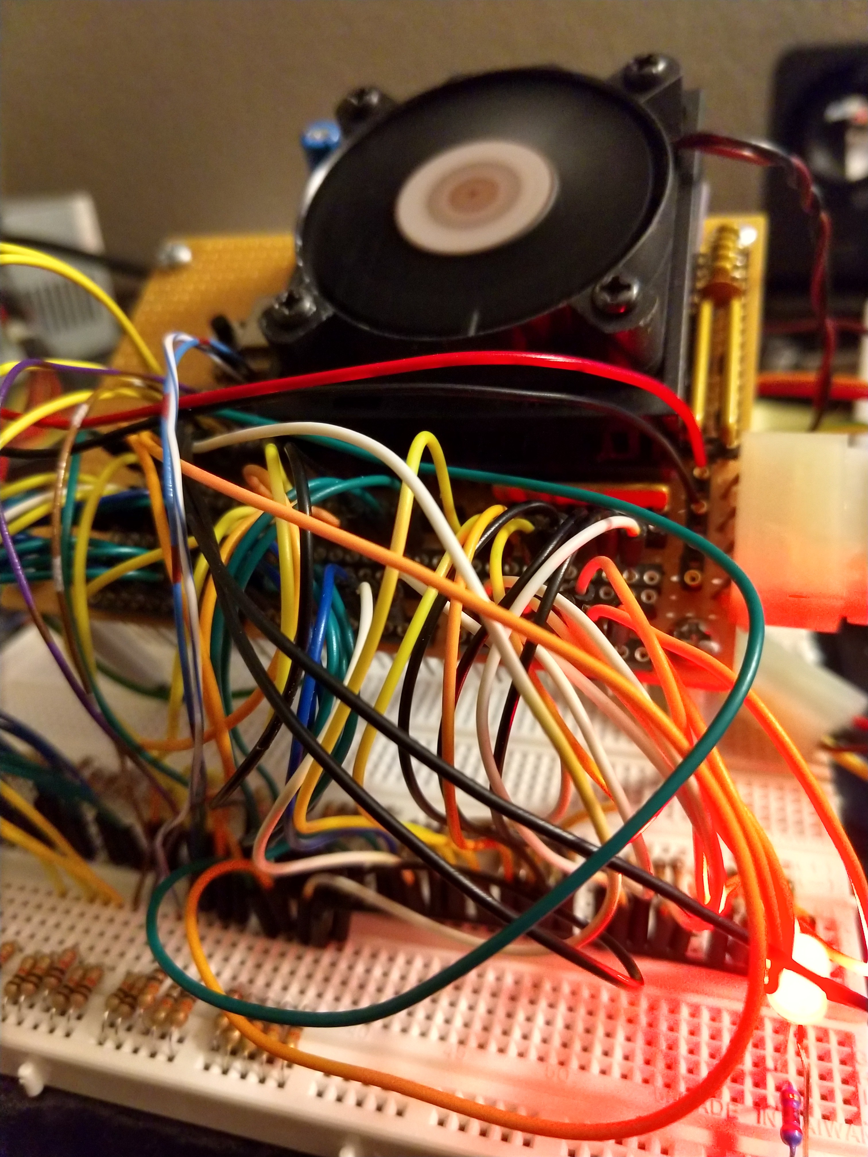
I chose to use a small, cheap protoboard and wire-wrap pins for easy prototyping. I worked ahead and added sockets for the 8 registers that I'll be using for first code, and wired them to the 64 data bus signals. This allowed me to easily plug in wires to run to a solderless breadboard where I installed pull resistors for the x86 NOP instruction (op code 0x90). This instruction is repeated 8 times to meet the Pentium's requirement that the entire 64-bit data bus be present for code read cycles.
Pentium has 23 input signals for interrupts, system management, cache control, and of course clock & reset. Obviously interrupts, system management, and cache can be ignored for simple systems, especially free run. A pull-up resistor is suitable for any active low signals, and a pull-down resistor for the active high signals. The only signal that will need to be asserted is the Burst Ready signal (BRDY) which indicates to the Pentium that an external device has valid data on the bus for a read cycle. Similar to the DTACK-grounded approach for the MC68000, BRDY can be grounded to immediately complete a bus cycle on the Pentium.
For my tests, I'm running the clock with a 25MHz can oscillator. This is below the specified minimum 30MHz/33MHz clock, but should still work just fine here. Reset does need a valid reset circuit though. Pentium requires at least a 1ms pulse on its RESET input following the initial rise of Vcc on power on. I prefer to use an RC timer with 74'14 Schmidt-trigger inverter for reset circuits. It's dead simple and I've found it to be very reliable.
Troubleshooting
Unsurprisingly, the first time I flipped the switch it did not run as expected. I had logic analyzer probes on the the Memory-I/O signal, Reset, Address Strobe, Vcc, and a few other signals. I could see Vcc rising, I could see high and low values on Reset. Instead of seeing Address Strobe going low to indicate the start of each bus transaction, It rose with Vcc and stayed there. No free run.
Initially, I had hoped to get away with just a pull-down resistor and switch on RESET. I didn't think a little switch bounce would be much of a problem. This did not prove to be a valid assumption. I had to go back and build a proper power-on reset circuit.
Even then, I was having trouble with excessive rise/fall times on the RESET signal. The 74HCT14 I'm using for reset should have rise/fall times under 15ns, but I was seeing somewhere over 100ns. I suspect the cheap logic analyzer might be at least partially responsible. When I finally stopped watching RESET, I started to see the first signs of life.
It turns out I had also omitted a single Vcc pin. I find it hard to believe that the one missing power input would have any significant effect on operation (given that there are 49 others), but perhaps it directly feeds some important function in the chip? I did actually encounter something like that with the MC68030, where different portions of the CPU (data/address buffers, control logic, etc.) were powered by specific Vcc/Ground pins. If such information is specified in the Pentium data book, I've not yet found it.
Current Status & Next Steps
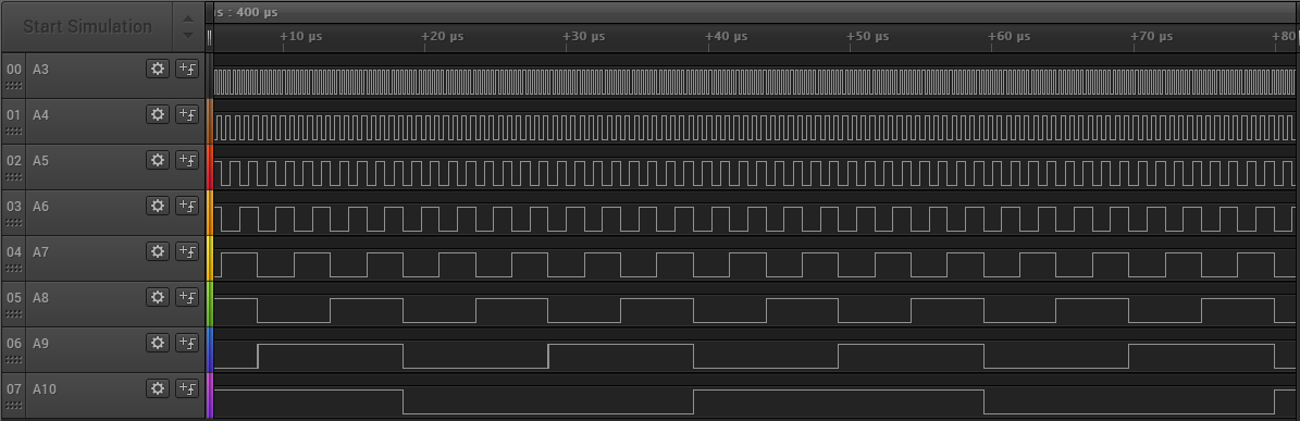
So right now, the CPU does free run ... for around 1.3ms before stopping.
Looking closely at the timing on the lower address signals, A3 (the lowest brought out on the Pentium) is oscillating at around 320ns. This is the expected rate for the CPU running at 25MHz — extrapolating from here, if it were brought out, A0 would be oscillating at the full 25MHz. The 8 NOP instructions the CPU is fetching at a time are being executed for each transition of A3. Extrapolating in the other direction, 1.3ms is right around the length of time the CPU would take to increment through a full 64k address segment.
At that point, the CPU halts, outputting an address ending in 0x138 (A[10..3] = 0b00100111).
It seems like an odd place to stop. I need to run a few more tests, see if it consistently stops at the same place, and the see what the rest of the final address is. So far, I have two clean captures — one from cold power on, and one from warm reset — and both ended on the same value after the same length of time. I also need to probe the output status signals to see if they give any indication of what the fault might be.
While I continue to troubleshoot the halting issue, I'll also be working on the sequencing logic for reading 8 bytes from an 8-bit flash ROM and storing them in registers to meet the 64-bit code read requirement. I've made a first pass through in Logisim just to get a feel for how it will work, but I'll probably be able to cut it down to just a few lines of VHDL.
As for right now though, I just love the utterly ridiculous sight of the Pentium heatsink and fan alongside a rats nest of prototyping wires.
Discussions
Become a Hackaday.io Member
Create an account to leave a comment. Already have an account? Log In.