 Yann Guidon / YGDES
In the source code of LibreGates, one can find a file named LibreGates/SRFF_simple.vhdl and this log explains its purpose, because it is well justified despite opinions of the contrary. The following is a summary of the discussions with @alcim.dev. Let's start by looking at the header:
-- file LibreGates/SRFF_simple.vhdl
-- created mar. août 25 02:51:59 CEST 2020 by whygee@f-cpu.org
-- version mar. sept.  1 04:02:57 CEST 2020 : LibreGates !
--
-- This is the basic version and the initial definition for
-- various Set/Reset Flip-Flops, defined by the precedence
-- of the control signals and their active levels.
--
-- Precedence  Set  Reset  Macro
--            level level  name  Mapped to
--      Set     0     0    S0R0   AO1A
--      Set     0     1    S0R1   AO1C
--      Set     1     0    S1R0   AO1, AON21
--      Set     1     1    S1R1   AO1B, DLI1P1C1, AON21B
--    Reset     0     0    R0S0   OA1A
--    Reset     0     1    R1S0   OA1C
--    Reset     1     0    R0S1   OA1, OAN21
--    Reset     1     1    R1S1   OA1B, DLN1P1C1, OAN21B
--
You already certainly know the basic Set-Reset Flip Flops and this file implements them, though at a very abstract level, such as:
architecture simple of S0R1 is begin Y <= '1' when S='0' else '0' when R='1'; end simple;
So there is not much to say on this level, it's plain and dumb. But there are 8 versions, each one of the 2×2×2 combinations of precedence (set or reset), active level for set and active level of reset. As the header notes, each of these versions can be implemented with more than one circuit. The example below shows how to make S1R1 in 3 different ways:
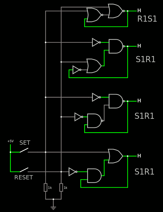
You can try the circuit on circuitjs with this link.
The first property of these "macrogates" is that they should not oscillate when both inputs are active (unlike some highly-frowned-upon circuit topologies that can be found here and there).
The second property is that there is a clear priority : one signal has precedence over the other. For example R1S1 at the top has the same active level but behaves differently when all switches are closed.
A third property is that even though they are represented here by 2 gates, they can also be implemented by a single composite gate, as listed in the header (using the A3P terminology though, YMWV).
This collection is an exhaustive taxonomy that is useful during design as well as optimisation, and the SxRy and RxSy definition is abstract enough that design is not too encumbered and optimisation is easy.
- During design, the designer knows that all combinations are possible so there is no restriction or constraint to get something done. There is a clear priority and the levels can be changed at will, knowing that an optimal implementation will be available later.
- During optimisation, there are two more benefits :
- the gate can be selected and changed to favour speed in the high-speed critical datapath, by selecting an implementation that has the least logic depth at the right place. The other input can come from a "slow circuit" with less of speed constraint, like an outside control or debug signal.
- the gate can also ease bubble-pushing because all level combinations are possible (2 inputs, one output, yeah that makes 8 combinations). Bubble-pushing can stop or start when reaching the SRFF gate, and be changed or adapted appropriately.
Of course this type of gate is not used in the heart of a high-speed circuit. This is necessary when clock domains meet and a signal must cross them, usually with some kind of handshake. It is particularly important for debug/monitoring/control/test circuits, as well as asynchronous I/O ports (for example with serial circuits where the clock comes from outside).
Debug circuits can become quite complex and this little meta-library provides the designer with enough flexibility to get things done right. It is up to the designer and upstream providers (ASIC PDK, FPGA...) to then map the metagate to the appropriate standard (or custom) cell.
One example is the R1S1 gate made of two NOR2 gates at the top. It is pretty optimal, transistor-wise and it can be mapped to an existing OAN21B gate. Now if this gate is used "like a lot", it makes sense to create a version of the OAN21B standard cell where the output is connected directly to one input. This saves a bit of P&R trouble because the feedback loop can stay inside the cell, saving routing resources.
One PDK can implement only the smallest and most efficient gates (such as made of NOR-NOR and NAND-NAND) and the synthesiser can "bubble push" downstream and upstream to get the desired function, but the user doesn't have to care much. The above file provides a high-level description that is enough to simulate and test the whole circuit and the LibreGates functions can handle these, when the "backwards" meta-gate is inserted in the feedback loop. This way, asynchronous circuits are not avoided or ignored or forbidden !
...
Update :
As you can test yourself there, only NOR2-NOR2 (R1S1) and NAND2-NAND2 (S0R0) give viable minimal latches. Minimal because both NAND2 and NOR2 use 4 MOS transistors each (in CMOS world). So in this context, a minimal SRFF uses 8 transistors. Combining NOR2 and NAND2 keeps the state stuck. So all the 6 other combinations must use inverters and/or bubble-pushing upstream and/or downstream.
For less optimal results, other more complex gates can be used, as listed in the header of the file. These gates use internal inverters and take a bit more resources (a few more transistors) but sometimes it is required. In the worst case a pair of more traditional gates can still be assembled.
....
Re-update :
Have a look at https://hackaday.io/project/27280-ygrec8/log/220111-a-semi-decent-output-port where SR latches are used.
Discussions
Become a Hackaday.io Member
Create an account to leave a comment. Already have an account? Log In.