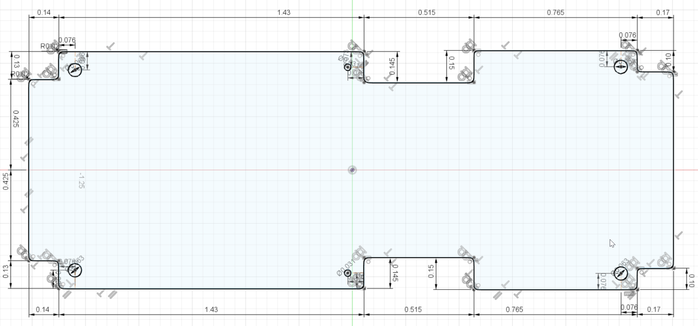
When I started capturing the board dimensions I made a lot of assumptions about the shape. As I progressed, however, I quickly learned that the exact shape of this board is surprisingly nuanced.
The cutouts were not of uniform depth and needed to be nearly perfect to ensure I could get the screw hole cutouts in the right locations. It took a few redesigns to get it just right.
Since there was no universal geometry I could base my work off of, I used a pair of calipers and measured around the board, using locations from my previous measurements as a base for my next ones (I'm sure I've broken a fair number of cardinal sins doing this, but since I have no classical training in CAD this is the best I can do for the moment). Regardless, I'm happy with how this turned out. After working all the way around and mirroring my design, I was able to draw a line bisecting the board that was 10 mills off from what my calipers reported. Considering the rough finish on the sides of the PCB and the fact my caliper's batteries were almost dead, I'm quite happy with this.
I'll order a blank test board once I've queued up enough PCBs to justify a order from JLC. There's plenty more to do in the meantime, like developing a circuit, sourcing a CMOS sensor, designing a mount for the camera module and USB receptacle, reverse engineering the audio/ LED status board, and checking the feasibility of manufacturing an aluminum USB C cover on the base to replace the Firewire one.
Stay tuned!
Discussions
Become a Hackaday.io Member
Create an account to leave a comment. Already have an account? Log In.