 Mitsuru Yamada
1. Address area and switches
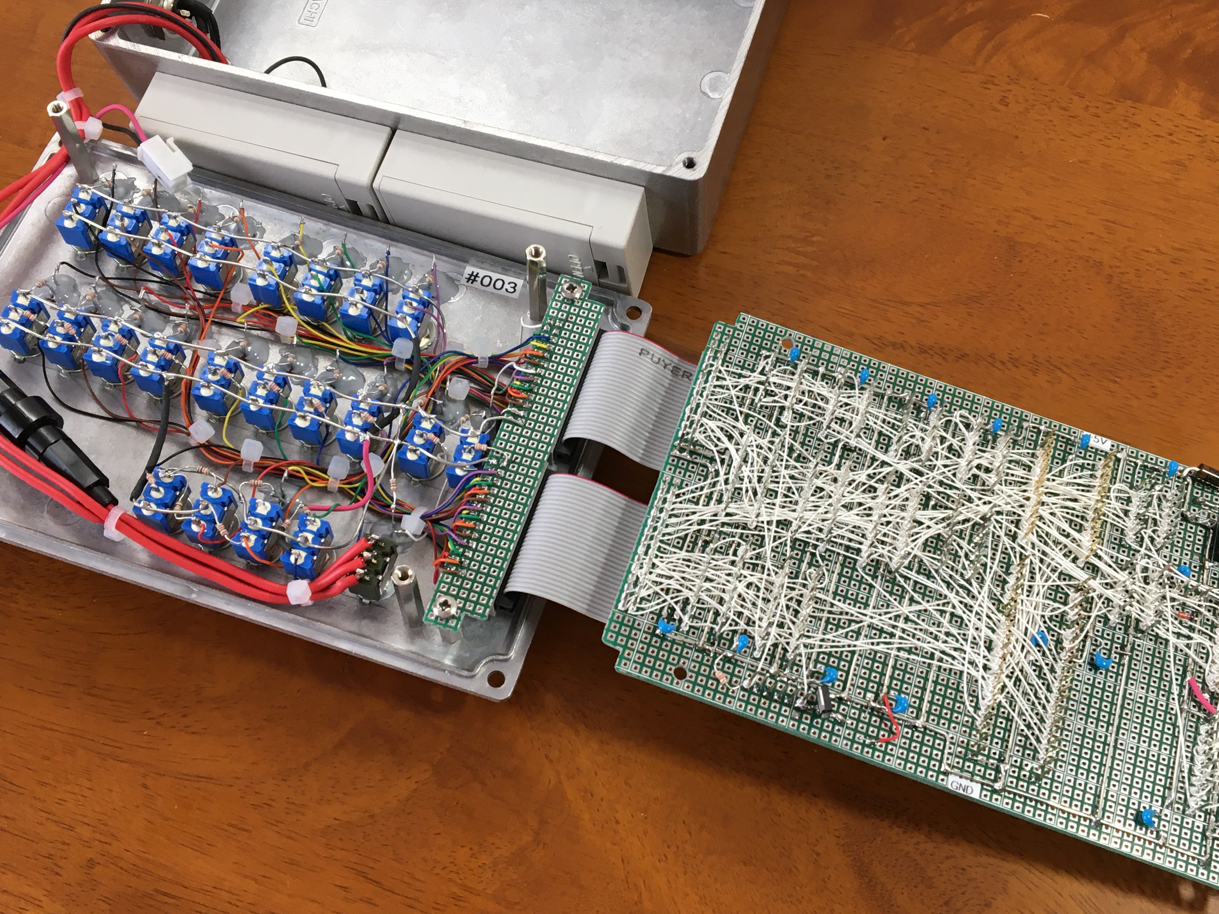
The operation panel has been simplified to realize the first concept, and the toggle switches for address setting are 10 bits. So, the memory space is only 1 kbytes. I thought that I could still execute a simple machine language program. Zero page is $ 000 - $ 0FF, stack area is $ 100 - $ 1FF, vector area is converted $FFFA - $FFFF to $3FA - $3FF and the rest are free areas.

2. Address LEDs
The LEDs for address display are also 10 bits, and the status of the address bus is always displayed. In the case of single step operation, the execution address of the instruction is displayed in sequence. Without this function, it is difficult to debug because you cannot see the runaway instruction in single step operation.
3. Data switches and LEDs
The data setting switches are 8 bits. The LEDs on the data bus display the data value of the memory for which the address is set when the CPU is stopped. If you operate the write switch at this time, the status of the data setting switch is written to the memory. When the RUN/HALT switch is set to the RUN side, the CPU goes from a halt state to normal continuous execution.
4. Circuit
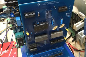
The external interface has an 8-bit parallel write port and a read port. The power supply is a four 1.2 V NiMH AA rechargeable batteries or an external 5 V power supply. The LSIs mounted on the board are R6502A for CPU and HM6116LP-3 for SRAM. Thirteen standard CMOS logic ICs configure a clock generator, 8-bit parallel port, address decoding, and Direct Memory Access(DMA) bus control as shown in the schematic to realize the second concept.

5. Circuit operation
The CPU halt state is performed by setting the ready(RDY) signal to low state, and the single instruction operation is performed by setting the RDY signal to high state until the SYNC signal becomes high state. In the halt state, the CPU IC1 continues to output the execution address to the address bus, so the address LEDs D2-D11 display the execution address. The address bus of the memory IC2 is disconnected from CPU by the 3state buffer IC4 and the Address switches S2-S11 are enabled.
When write switch S1 is operated, data switches S12-S19 are connected to the memory IC2 though 3state buffer IC7, and write enable signal is applied to the memory. The RDY signal is set to high state during the reset. Otherwise, the R6502A would not have a correct reset sequence. It seems that this control is not necessary for R65C02.
6. Making
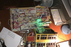
18 cm x 12 cm x 5 cm aluminum die-cast housing was used to realize the third concept. It was processed with a hand drill and files. Wiring on the universal board was done by wire wrapping. The switches and LEDs are mounted on the panel of the housing and connected to the main board with two 26p flat cables. First, I made one prototype. Then I made 3 more of the same ones by hand. The making time per unit is about 60 hours. So, including the operation test, it took a total of 4 months.
7. Results
I was able to make a small portable stand-alone 6502 machine language computer. Memory writing with DMA and single instruction operation worked fine. If it was a machine language program of several tens of bytes, I could easily input it and check the operation. However, in the case of a long program, it is necessary to be careful not to runaway due to a bug. This computer does not implement a memory protection feature for simplicity. The power consumption is 5 V x 230 mA = 1.2 W and the battery lasts about 5 hours. Finally, I'm happy to give this computer to three acquaintances.
8. Example programs
Two simple program examples are shown below. The SIMPLE_TEST-1_1 is to increment a memory value, and the following video, the KNIGHT_RIDER-1_1 is to use a programming timer to move the lighting of a row of LEDs connected to the parallel port. As an example of a program with full memory capacity, a fixed-point calculator...
Read more »


 ammarbhayat28
 Craig
Craig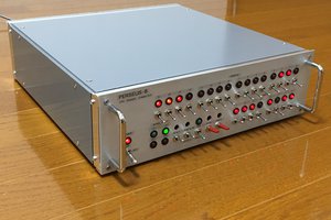
I really like such projects,
Since I teach Computer Science at a Highschool in Austria (pupils aged 15-18 years) (http://www.gymnasium-am-Augarten.at) I plan to build it myself as an example how computers are programmed at the lowest, electronic level to give an impression what a compiler really does ;-)
Edgar