 David Reiss
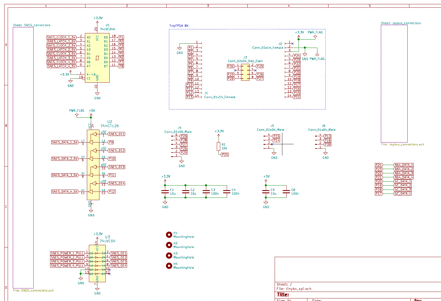
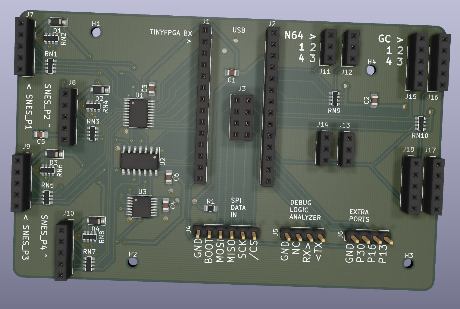
The centerpiece of this board is a TinyFPGA BX, mounted on female 0.1" headers.
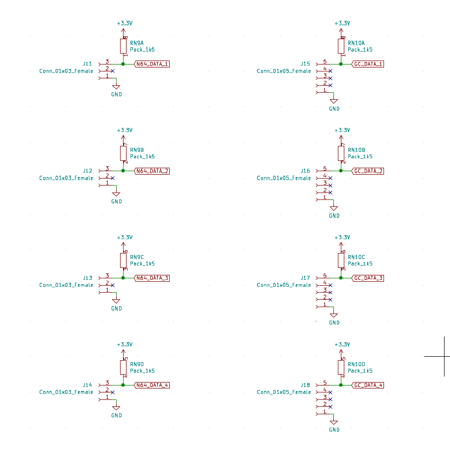
The connection to the N64 and GameCube is very simple: just a direct connection to an FPGA pin, with a 1.5 kOhm pull-up. (I measured a similar value in an authentic controller.)
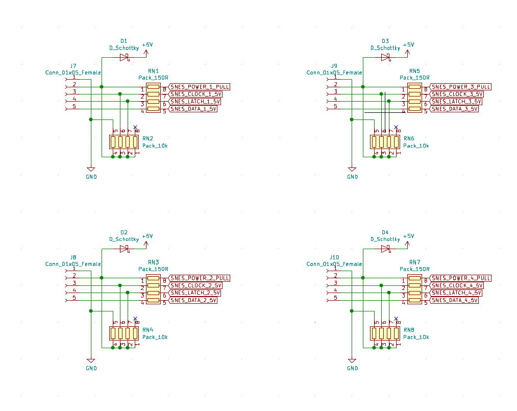
The connection to the NES/SNES controllers is more complicated. First, because these consoles operate at 5V, I need level shifting: 74LVC245 on the input and 74HCT125 on the output. I observed some bounce on the input signals while working on a breadboard, which is problematic for the clock. Nexperia's datasheet for the 245 says it has "Schmitt-trigger action at all inputs". It doesn't document a specific hysteresis value, but it should help a bit. I'm also using 150 ohm terminating resistors, which helped dampen the signal in my experiments. The SNES internally uses a 100 ohm series terminator with a 330 pF capacitor behind it, but I didn't really want to add 8 extra caps to this board. Maybe for revision 2.
It's not clear whether I really need push-pull outputs for the NES/SNES data lines (since the consoles have internal pullups), but I decided to use them because the original controllers have them. I pass the power pin for each console through a 74LVC04 inverter to control the /OE lines for each data output so I'm not driving an external pin unless the console is actually powered on. I don't have an on-board 5V supply. Instead, each NES/SNES port passes its power through a Schottky diode to the 5V rail.
The input data lines are weakly pulled up by the power line from the same console connector. The power line is weakly pulled *down*, so the data lines idle low when the console is powered off.
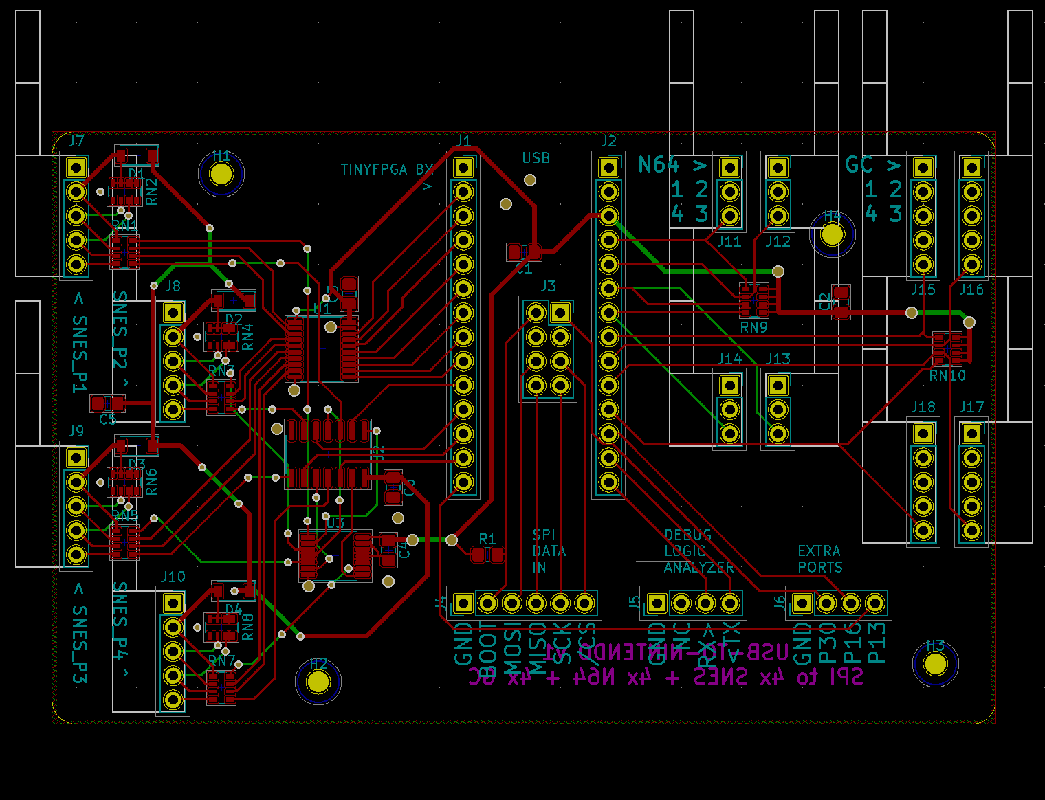
I tried to keep most signals on the top copper. There are several bottom traces near the NES/SNES side. I tried to reserve them for low-speed signals and power. The clock signals are the most sensitive, and they all stay on top. I'm a bit worried about cross-talk between the clock and data lines since they transition at about the same time and the data transition could possibly cause the clock to bounce. Fortunately, the latch line is always between them.
Besides the controller ports, I have external ports for the Raspberry Pi, an integrated logic analyzer (UART), and the unused FPGA pins (possible expansion for NES/SNES Classic).
I don't have diode protection on any of the external pins. I'm not sure how important it is.
Discussions
Become a Hackaday.io Member
Create an account to leave a comment. Already have an account? Log In.