 Bharbour
Overview
The simplistic circuits shown in old books for driving step motors work fine at very low step rates. When the step rates start to increase, the motor torque output falls off very quickly. There are two reasons for this:
1) Motor back EMF generation.
2) Motor winding inductance.
Back EMF is a "feature" seen in most DC motors and step motors. When the coils move through a magnetic field, they generate a voltage. In the case of step motors, the magnetic field moves and the coils are stationary. The polarity of the generated voltage is opposite the polarity that would be required to drive the motor in that direction. The result of this is that the net voltage across the coils is the input voltage - the back emf voltage. The faster the motor turns, the less voltage availible to the coils.
Motor winding inductance is just the physics of the motor construction. The number of turns in the coils of wire and the magnetic structure of the motor set the inductance. Inductance opposes changes of current. Skipping the calculus, assuming that the drive voltage is constant, the current rises at a fixed rate. As the step rate increases, the amount of time for the current to rise in each step gets shorter so the motor current drops off. For a step motor, the net voltage across the coil does not stay constant as the speed goes up, the net voltage across the coil drops from the back EMF generated.
Raising the input voltage will overcome both of these problems, at the cost of creating one new problem. The new problem is that when the motor is stopped or moving slowly, the higher voltage across the coils will drive too much current and the motor will heat up rapidly. The solution to this problem is to regulate the current into the motor.
The inductance of the motor makes it fairly easy to regulate the current. When a voltage is applied across an inductor, the current rises linearly with time. If you measure the current flow and turn off the voltage when the current rises to the desired level, the average current is pretty well controlled.. The rest of the step motor driver system already supports switching the voltage on and off to each coil rapidly, so all that is needed to regulate the current is to install a low value resistor between the transistors on the low side and ground, and a comparator to sense the voltage across that resistor. The resulting circuit is called a chopper drive circuit because of the on/off action of the current regulation.
When the current rises to the desired value and the comparator switches off the voltage supply to the coil, the current already flowing circulates through the motor coil and the diodes protecting the transistors. These diodes may be internal to the transistors in the case of MOSFETs or external. It is not uncommon to use external diodes to help the internal diodes (called body diodes) on MOSFETS because the body diodes tend to not be great diodes. In operation, the current circulating takes a while to decay, so it does not drop to zero instantly when the supply transistor switches off. When the current drops below the set value, the supply side transistor turns back on. The current cycles above and below the desired value fairly closely.
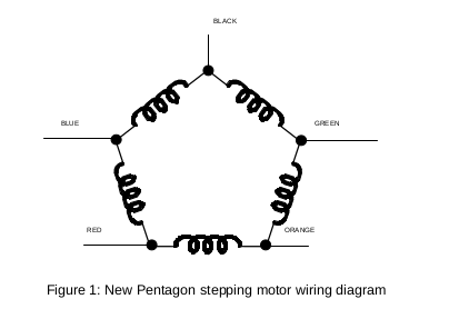
As mentioned in the introduction, these motors are 5 phase motors. The drawing below shows the configuration of the windings (TM Oriental Motor)
None of the step motor driver chips that I saw will support this configuration other than the ones sold by Oriental Motor.
There is good documentation on the MPJA web site for the motors and drivers, so I designed the step generation logic in 74HC logic. When I was done, the implementation would have been at least 12 chips. After adding the power and gate drivers, this was starting to look like a medium sized 4 layer board which would be expensive. As a way to reduce board area, I found some little Xilinx CPLD (Complex Programmable Logic Device) parts that would be large enough for the step generation logic. This choice saved the board later, when I discovered problems in the step generation logic.
Hardware Details
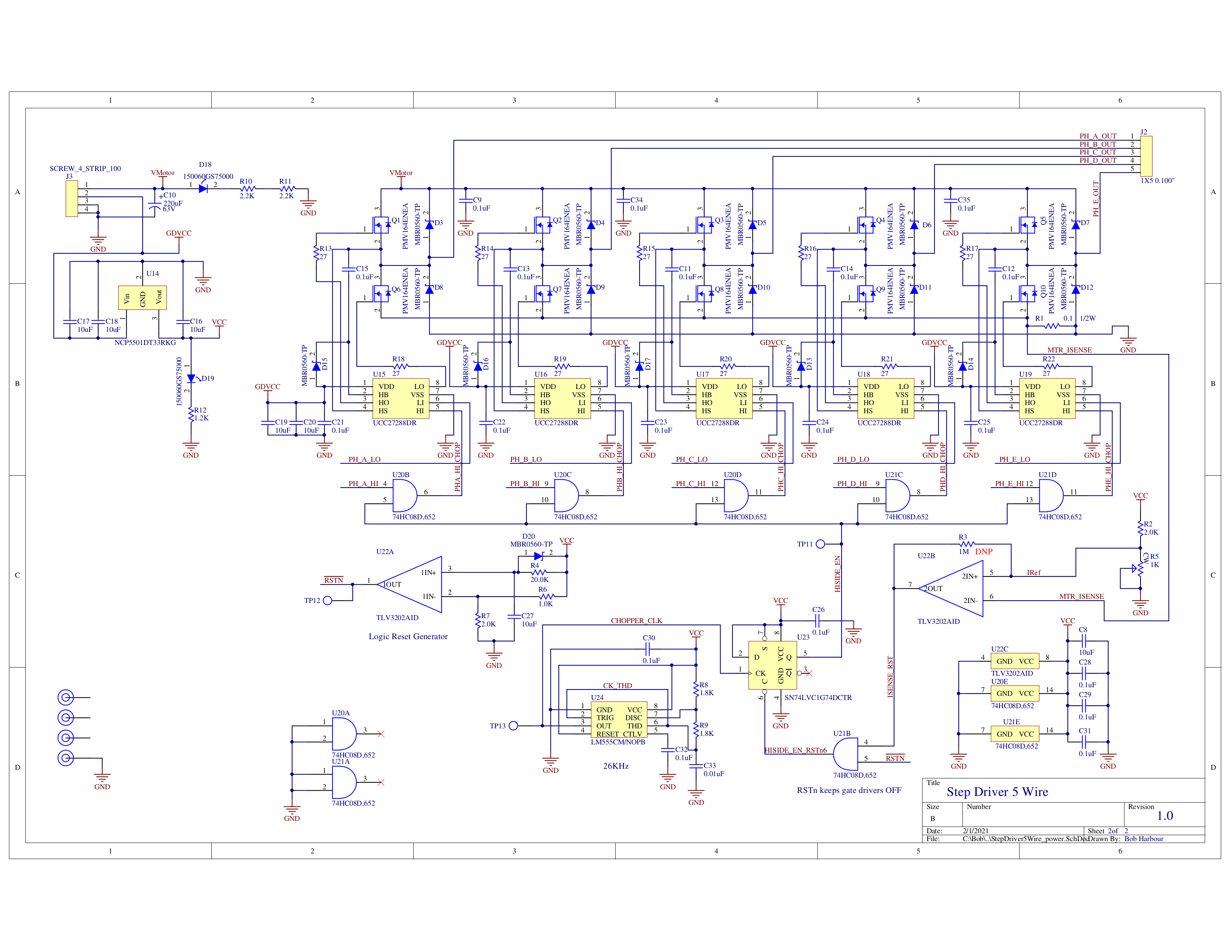
Here is the power section schematic.
Power comes into the board through J3 in the upper left corner of the schematic. The motor voltage may vary from 10V up to about 22V, so it is kept separate from the control power. The gate driver chips want 10V to provide a controlled gate supply voltage for the high side MOSFETs. Power for the logic also comes off the gate driver VCC input through a Low Dropout 3.3V regulator chip. The logic power is only a few milliAmps, to the regulator heat dissipation is minimal.
To the right of the power input is the row of 5 coil driver circuits. Each coil driver circuit has the high and low side N Channel MOSFETs, two SCHOTTKY diodes to control the inductive currents from the coils and a gate driver chip that translates the logic level control signals into the levels required to drive the MOSFET gates. Output to the motor coils are through J2 in the upper right coner of the page.
All of the low side MOSFETs are connected to a single rail (MTR_ISENSE) that returns to ground through a 0.1 Ohm current sense resistor (R1). The MTR_ISENSE voltage also goes to the - input on a voltage comparator chip (U22B). Resistor R2 and pot R5 are used to develop the setpoint voltage for regulating the motor current that goes into the + input on the comparator U22B. This is not a terribly precise thing, so the logic supply voltage is stable enough. When the motor current rises, the voltage on MTR_ISENSE rises proportionally. When the voltage on MTR_ISENSE rises above the setpoint voltage, the output of the comparator goes low, clearing the D flip flop U23. The output of U23 is used to enable the high side control logic. If U23 's output is low, the high side MOSFETs are turned off.
With the D input on the D flip flop (U23) tied high all the time, as long as the comparator (U22B) output is high, the output of the D flip flop will go high every rising edge of the chopper clock signal that runs at about 26KHz. The purpose of the D flip flop in this circuit is to provide some order to the current control logic. The AND gate U22B placed in the path between the comparator and the D flip flop clear input just insures that the high side MOSFETs are switched off until the reset signal goes inactive.
Phase sequencing signals from the CPLD on the other page come into the power section in the middle of the page. High side phase enable signals go into the AND gates to combine them with the current control signal. Low side phase enable signals go directly into the gate driver chips.
The row of AND gates between the D flip flop (U23) and the high side gate driver inputs could probably be incorporated into the CPLD logic. I left the discrete gates in place until I could verify that the gate control signals from the CPLD were well behaved during the power up and reset process.
Comparator U22A generates the power up reset signal RSTN. Capacitor C27 charges through resistor R4 when the power is applied to the logic circuits. The reference voltage for the comparator comes from the voltage divider R6 and R7 giving about 2/3 of 3.3V. It will take about 200mS for the capacitor voltage to rise above the reference voltage, which will allow the RSTN signal to go high. Diode D20 will discharge the capacitor if the logic power supply voltage goes low for a short period of time. This is to insure that the reset signal goes active after a short power glitch.
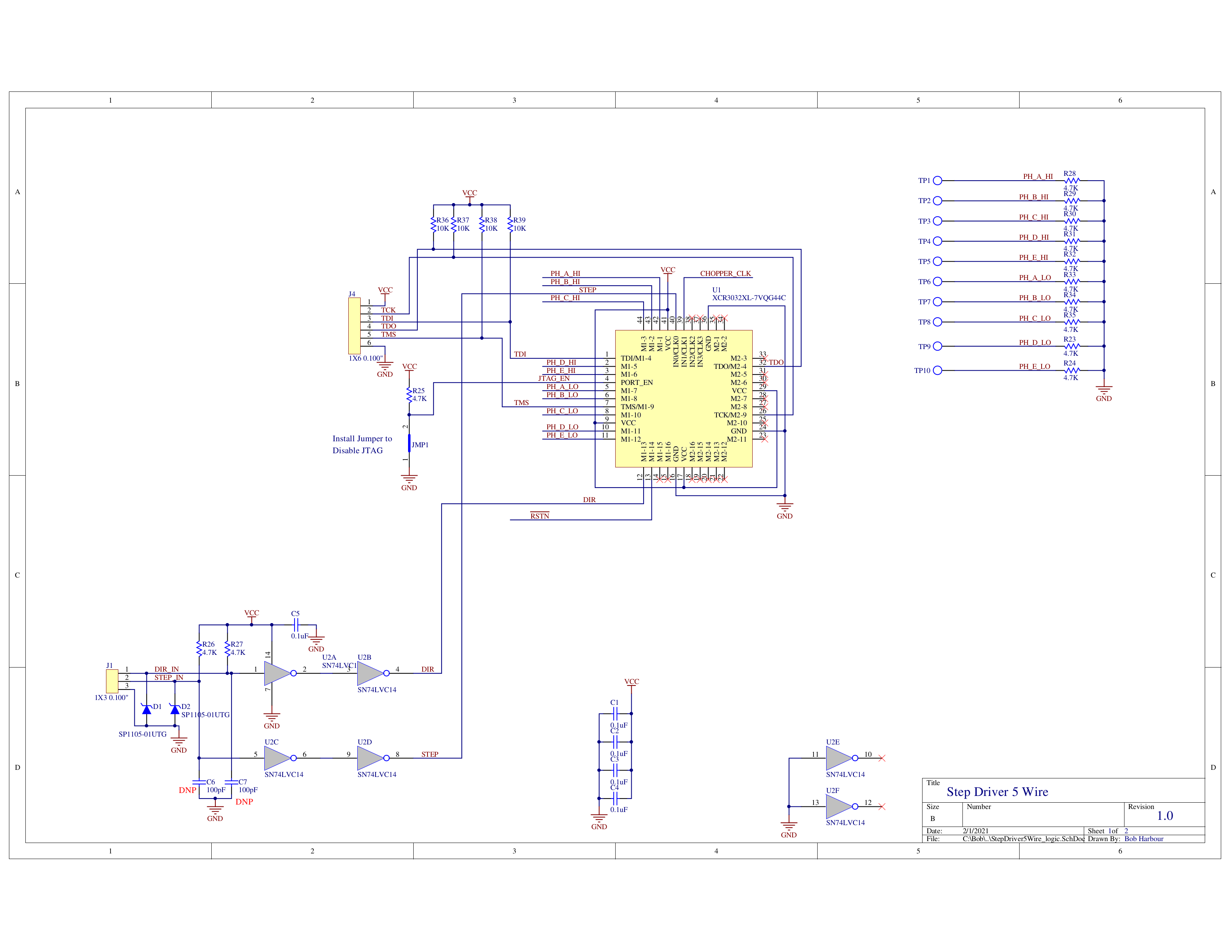
Here is the schematic with the step generation CPLD. The CPLD is in the center of the page. The JTAG connector for configuring the CPLD is just to the left and the CPLD. A USB to JTAG dongle interfaces Xilinx's tool chain to the hardware. This step only needs to be done once when the board is built or if the design of the sequencer is changed in the verilog file.
Step and direction control signals enter the board and go through ESD protection and some Schmidt Trigger inverters to clean up slowly transitioning signals or noisy signals. There are sites for filter capacitors on the step and direction signals, but they are not populated.
In the upper right corner, there are pull down resistors and test points for all of the CPLD outputs. When a CPLD first powers up, there is a short period of time while the internal logic gets configured. During this time, the outputs are all pulled high by weak pullup "resistors". Having all of the control signals high at the same time would cause the hi side and low side output transistors to turn on simultaneously with REALLY bad results. The weak pullup "resistors" are about 40K - 60K Ohms, so the 4.7K pull down resistors are strong enough to keep the control signal outputs low during the configuration phase, and weak enough to present minimal load when the logic is active.
Only two signals come from the power section of the schematic into the CPLD, the active low power up reset signal (RSTN) and the chopper clock signal (CHOPPER_CLK).
When the system powers up, the flip flops in the CPLD are in random states. The RSTN signal stays low for a time longer than the time required for the CPLD internal configuration to complete. When the internal configuration is done, the step generation sequencer is properly initialized by the RSTN signal which goes inactive (high) a short time later.
The CHOPPER_CLK signal was routed into the CPLD, but is not used at this time.
On the power section of the schematic, each motor coil input has an N Channel MOSFET connected between the motor power rail and the coil input (referred to as the high side driver) and another N Channel MOSFET between the motor coil input and the motor ground rail (referred to as the low side driver). Since this is a 5 phase motor, there are 5 pairs of these MOSFETs.
Output signals from the CPLD consist of 5 pairs (high side and low side) of switch control signals. Test points are included on these signals for debugging purposes.
Details on the Verilog code used to generate the step sequencer are in the first log file.