There are multiple implementations of such converters for high power applications both in isolated and non-isolated versions [https://www.ti.com/lit/ug/tiducs2b/tiducs2b.pdf] [https://www.ti.com/lit/ug/tidud04/tidud04.pdf] . Quite often in my battery powered project I face a need to develop both a battery charger and the converter stabilizing the battery voltage. The possibility of joining those two converters allows for savings on power elements and size. I wanted to try to develop experimental board to test different current measurement circuits and try to push the limits of maximum power. In this article I will try to present how to build a simple bidirectional converter with fast primary current feedback loop and digital secondary voltage feedback all implemented with small 8bit microcontroller.
Topology
In presented design I’ve decided to join two classic non-isolated topologies the buck and boost converter. In this configuration the converter allows for transfer of energy between two voltage potentials in both directions.
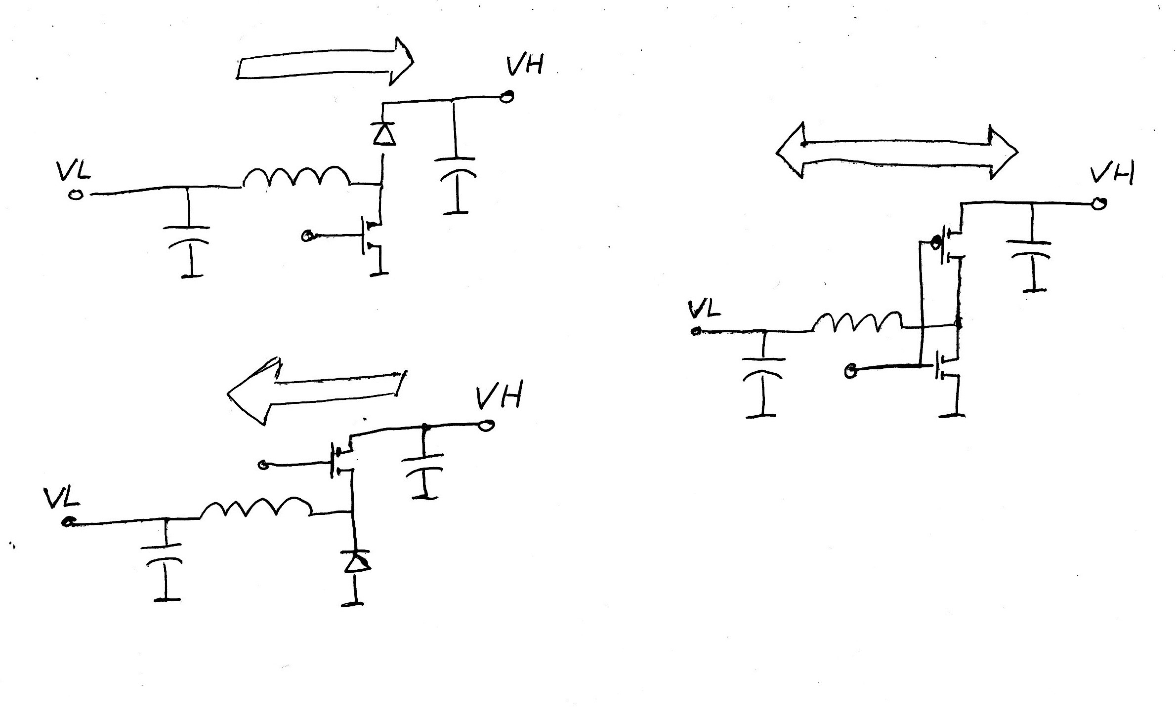
In such converter control of current flow is not only dependent on the PWM signal but also on the ratio of input voltages. Creation of feedback loop which only maps input voltages to the PWM signal would not only be difficult but also hard to stabilize. Also it would omit control of the current where current is one of the most critical parameters in charging and discharging of batteries. Probably because of that problem most of the mass produce converters for charging include feedback loop measuring current flow trough small resistor in series with the power inductor. This arrangement allows to measure current rise and fall at each cycle of the converter. Considering different possibilities of measuring that current I sketched following schematic.
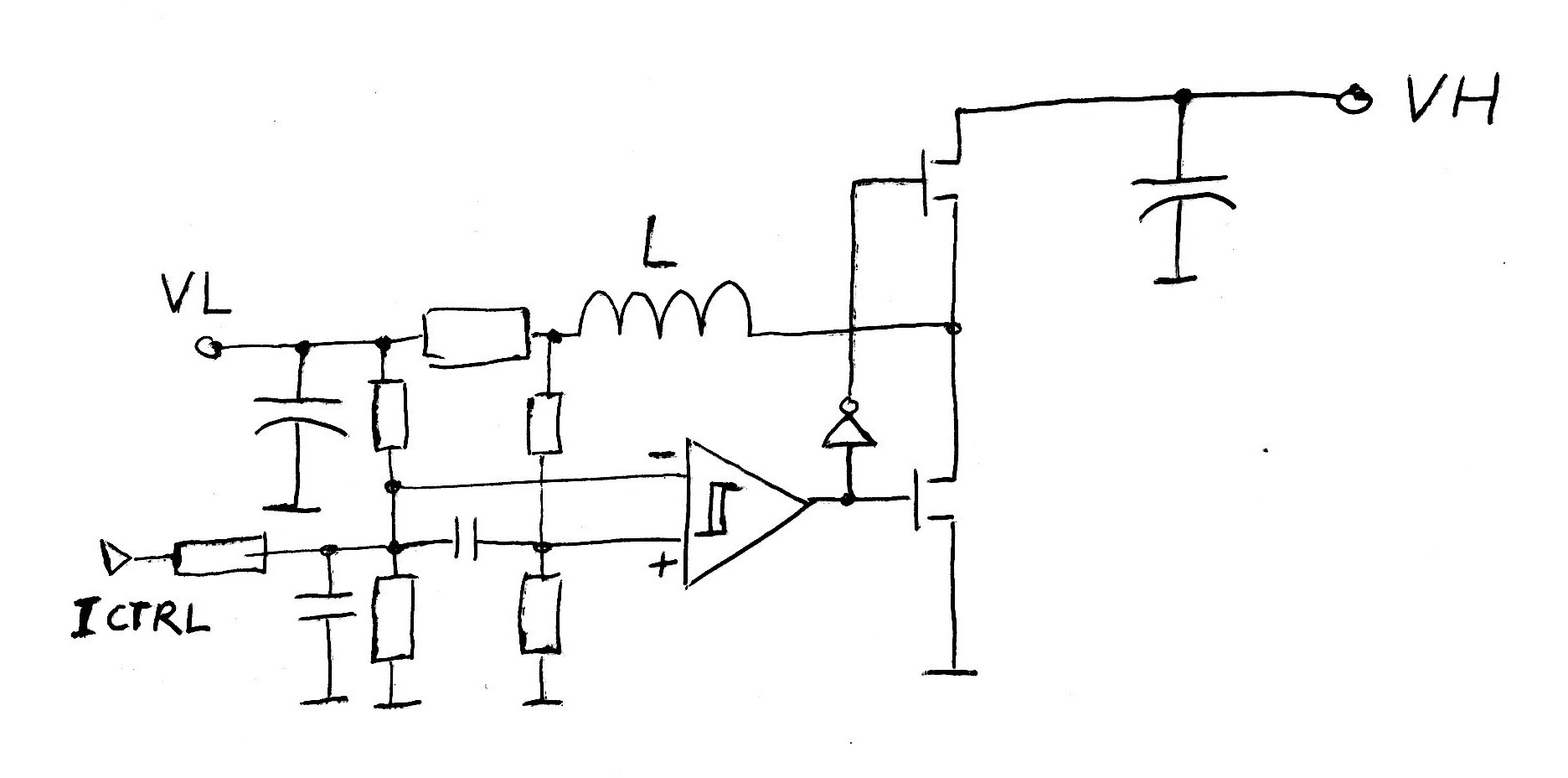
In presented circuit the main feedback element is the voltage comparator with hysteresis. By defining the converter phase and the state of main transistors it determines the cycle of increase and decrease of current in the main inductor. By simultaneously monitoring the current in the inductor trough the feedback resistors it limits the maximum rise and fall of that current. In this combination a negative feedback loop is created which creates cycle-by-cycle oscillations maintaining the inductor current within predefined range. The oscillation frequency is not fixed and it depends on inductor and resistors values, input voltages and and comparator hysteresis. Although the converter oscillates, in it’s default state the average current flow trough the inductor is null and no energy is transferred. Such oscillations maintain inductor in continues conduction state which might appear wasteful because of elements parasitic RI losses but surprisingly in presented circuit such losses represent only around 1Watt. While the comparator maintains the inductor current within predefined range additional control input (Ictrl) injects offset to the current measurement forcing average current to deviate. This allows the control of average current flow between input potentials and creates a abstraction block of voltage controlled current source.
Basic design
The main obstacle in designing bi-directional
converter is not
only a need for
controlling the voltages at the input and output but also the
decision of direction and amount of
current flow. That is why most design are
based on a digitally
implemented feedback loop inside a
microcontroller or a
dedicated DSP. To simplified my design both
in circuit and in software
I decided to use a simple
8bit microcontroller, consciously
sacrificing final precision and reaction speed for cost and
simplicity. I decided to use the Attiny1616
because I contained all necessary peripherals in a
simple package. Bellow is a diagram of the
converter design in it’s
initial form.
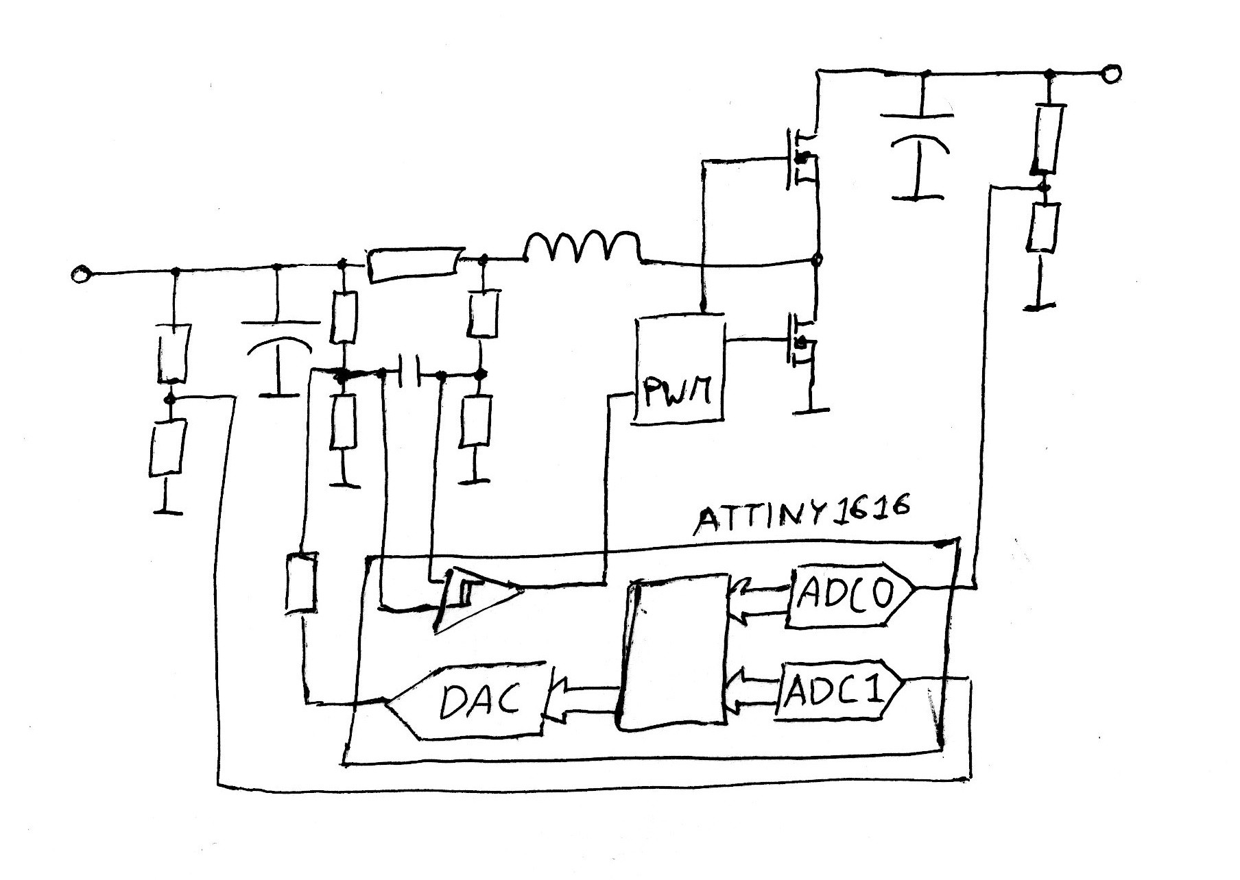
As I mentioned the main feedback loop creating oscillations and controlling inductor current is based on comparator with hysteresis. Using the build-in comparator allows for software level control over oscillations, hysteresis and starting and shutting down of the converter. Responsible for injecting the offset controlling the current is a build in 8bit digital to analogue converter. While two 10bit analogue to digital converters sample input and output voltage at 96ksps. With that frequency the code responsible for main feedback loop is also serviced. In this design the first working prototype was build but it showed that the weakest point was a inductor current measurement technique.
Sensing of inductor current
The most important part of this design is the method of sensing inductor current. The main challenge of this part is the pressure to reduce the current sensing resistor to the smallest value to limit power losses while simultaneously be able to still sense the high bandwidth of the signal reaching up to 500kHz. Additionally due to high side sensing the sensing signal has a wide and noisy common mode voltage which has to be rejected. I’ve decided not to use operational amplifiers for this part to simplify the design and avoid problems with its power supply. Below I present the few tried circuits and deliberate on their positive and negative aspects.
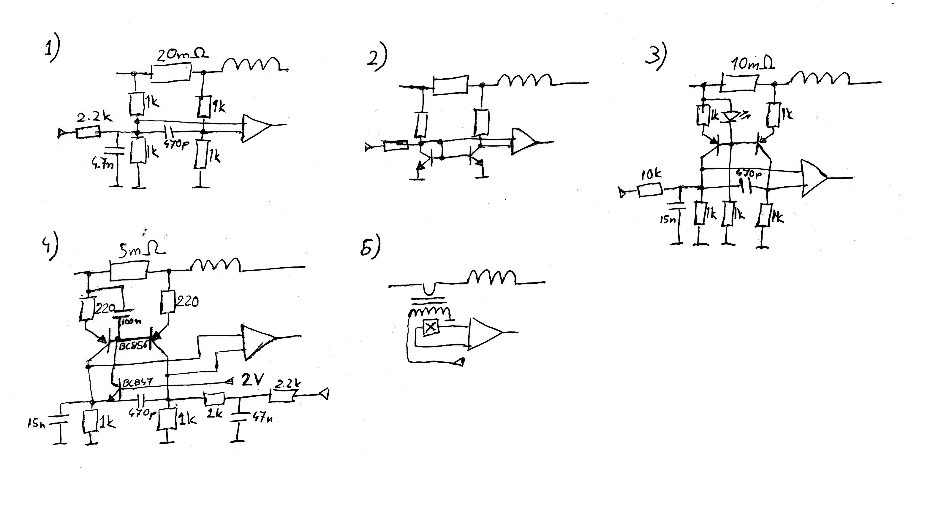
The first solution was to use simple resistor dividers. That solution allowed for the output voltage to extend above the comparator (microcontroller) power supply but it simultaneously divided the sensing signal. It also created problem when injecting offset into the node with potential varying with common mode voltage. This solution was the simplest and works good in converters with low voltages and power.
Second solution was to use a current mirror. This solution failed due to great intrinsic offset and small bandwidth. Unfortunately this solution is still visible in supplied schematics.
The third solution was to use two PNP transistors as common base amplifiers and bias the common base with small red LED. Although the output voltage was slightly dependent on common mode voltage and temperature this solution works great with common mode voltages between 3V to 20V. This solution successfully “copies” the sensing resistor voltage drop back to ground potential but does not create any amplification.
The forth solution was an improvement on the previous one. It used additional NPN transistor for active biasing of common PNP transistors base. This allowed to erase the effect of temperature dependent base emitter dropout voltage in PNP transistors and decrease emitter resistors to achieve amplification. In this design I was forced to inject offset to the other branch which limited the effective amplification of sensed signal to only 2. The converter presented in this project uses this solution.
The last solution which is still in the stage of idea is to create a copy of an oscilloscope current probe. The solution would use a Hall element to sense the current deviations and dictate the oscillations while a winding of high ratio would be used to inject the controlling offset.
I’m also open to proposition on how this part of the converter could be design.
Digital feedback loop
By basing the primary feedback loop on inductor current this part of the system can be modelled as a current source supplying capacitor and variable load resistor. Since such a system has only a first order response and does not experience “inertia” the secondary voltage feedback loop can be a very simple bang-bang controller. I decided to capitalize on fast response of bang bang controller and maybe worst regulation and tracking compared to more sophisticated but slower controllers. Bellow I present a simplified pseudo code of the secondary voltage feedback loop controller.
If((BusVoltage<12.0V)&&(BatteryVoltage>5.6V)) //Energy supply mode
    SupplyMaxCurrent();
Else if((BusVoltage>13.0V)&&(BatteryVoltage<8.4V)) //Battery charging mode
    SinkMaxCurrent();
Else
    MaintainNullCurrent();
Even this simple feedback loop executed with ADC sampling speed of
96kHz consumes 45% of microcontroller computational cycles. This
implementation shows how two Lithium cells (5.6V-8.4V) can be
connected to 12V bus. When the bus voltage falls bellow 12V the
converter supplies power when the voltage exceeds 13V the converter
starts draw energy to charge battery. Additionally the feedback code
maintains battery voltage and current between safe limits preventing
over charge and discharge. In ideal scenario such controller would
create very intensive current surges but in reality the ADC signal
contains a lot of noise which dilutes the controller response. This
creates a type of pulse density modulation at the output.
Additionally capacitor at the DAC output smooths out overall system
response.
Circuit construction
I’ve attached the schematics and PCB design in the supplementary materials but some of the elements are missing values and the current sensing circuit has been modified. In this paragraph I’ll try to summaries the values of main elements. I believe that most elements or their substitutes can be easily source at reasonable price.
Inductor: Core MICROMETALS T106-52, 6 turns 64x0.2mm, ~3uH ~2mOhm
Capacitors VL: 4x2200uF_25V, 3x2.2uF_X7R_50V, 3x100nF_X7R_50V
Capacitors VH: 4x1000uF_35V, 3x2.2uF_X7R_50V, 3x100nF_X7R_50V
Mosfets: 3xBUK7Y12-40EX, 2xBUK7M12-60EX
Current Sens Resistors: 2x10mOhm
Mosfet Driver: MIC4102YM
Microcontroller: Attiny1616
Supplementary Circuits: 1x Voltage reference for ADC REF3020, 2x current/voltage/power sensors INA219, Display OLED SSD1306 128x64
Results
The main current loop of the converter naturally oscillates at 200-400kHz. The secondary voltage feedback loop regulates voltage within ~0.2V precision. The converter flawlessly limits the current and automatically switches between supplying and drawing of the energy. The main limiting factor in increasing power is elements ability to dissipate heat. While testing circuit with only passive cooling and testing elements by only organoleptic means the converter was capable of maintaining 13A of current at low voltage side which equals to around 90W of power and in short term (5min) sustain 20A (140W). (Assuming a 7.2V battery connected to the low voltage side). In theory the converter could transform higher powers at higher voltages but I haven’t tested it. The energy losses were mostly contained between 2W to 7W depending on the load. At ideal point efficiency could reach 96% but it mostly circulated around 90% or even 80% at lower powers. When calculating efficiency I included power consumption of all axillary elements like power sensors and display. So far the only design flow is unanticipated mosfet driver under-voltage lock-down which requires high voltage (8V) to start the converter into action. Bellow few shots from converter performance tests. All test were done with X1 probe and voltage division seen on the knob.
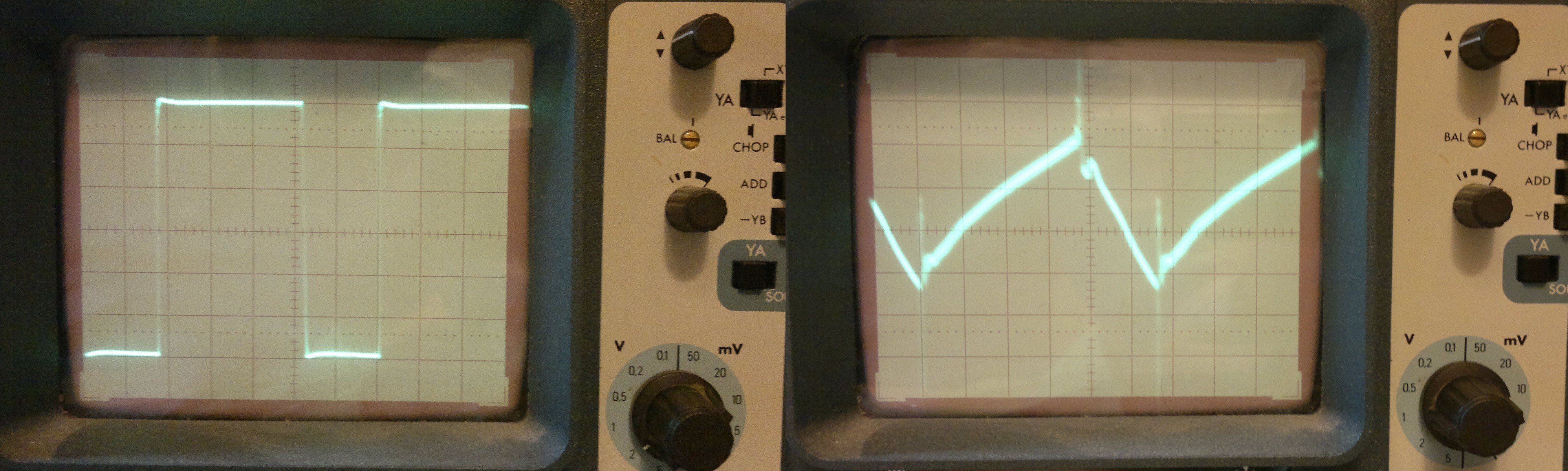
First is the shots of inductor current and voltage at normal oscillations (200kHz).
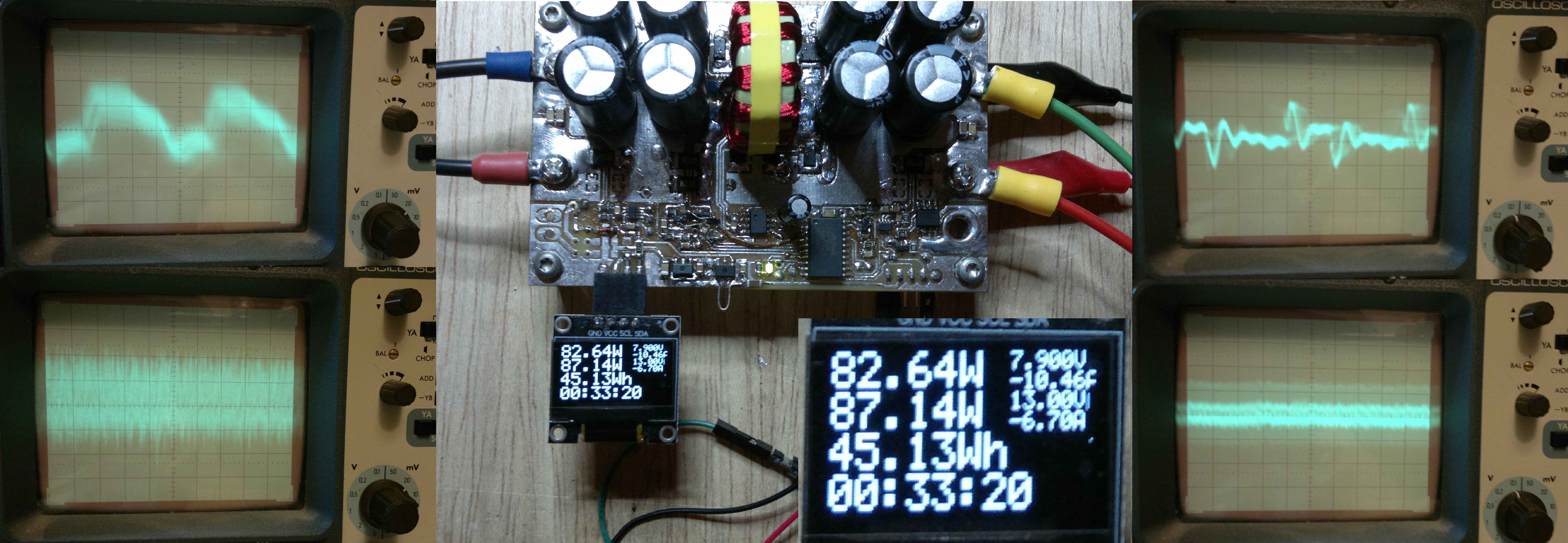
Converter in battery charging mode, the display show the charging parameters while oscilloscope shows the input and output ripple.
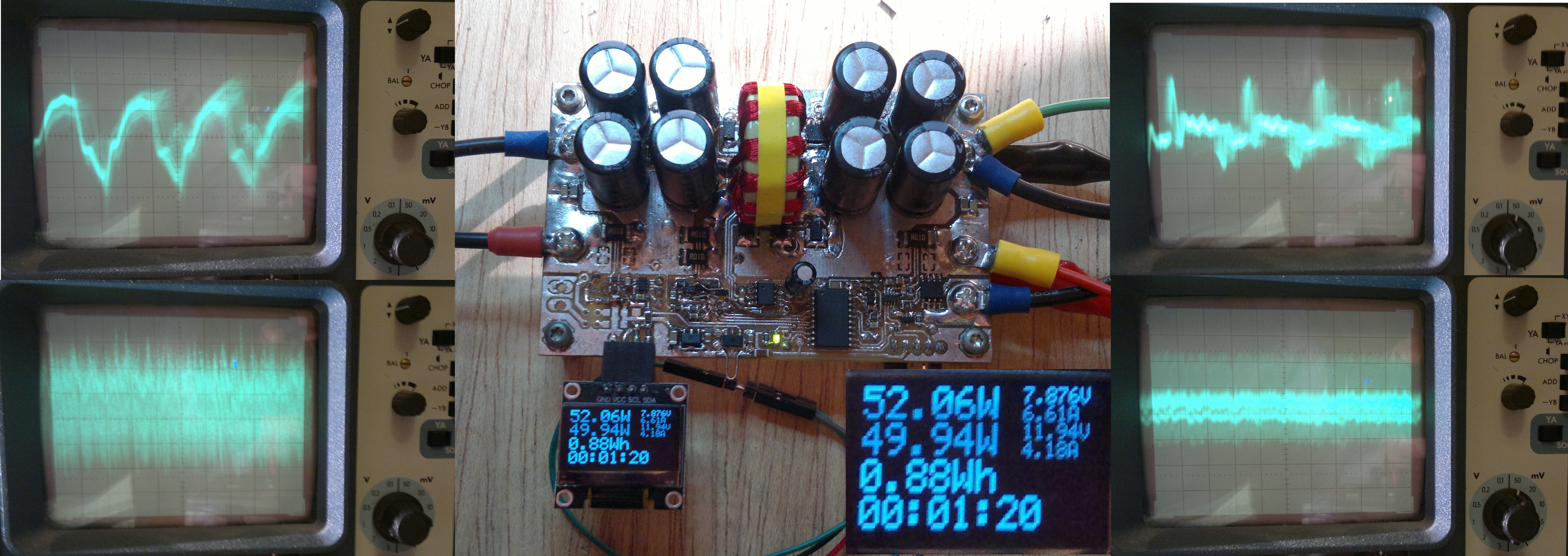
Converter in energy supplying mode, the display show the supply parameters while oscilloscope shows the input and output ripple.
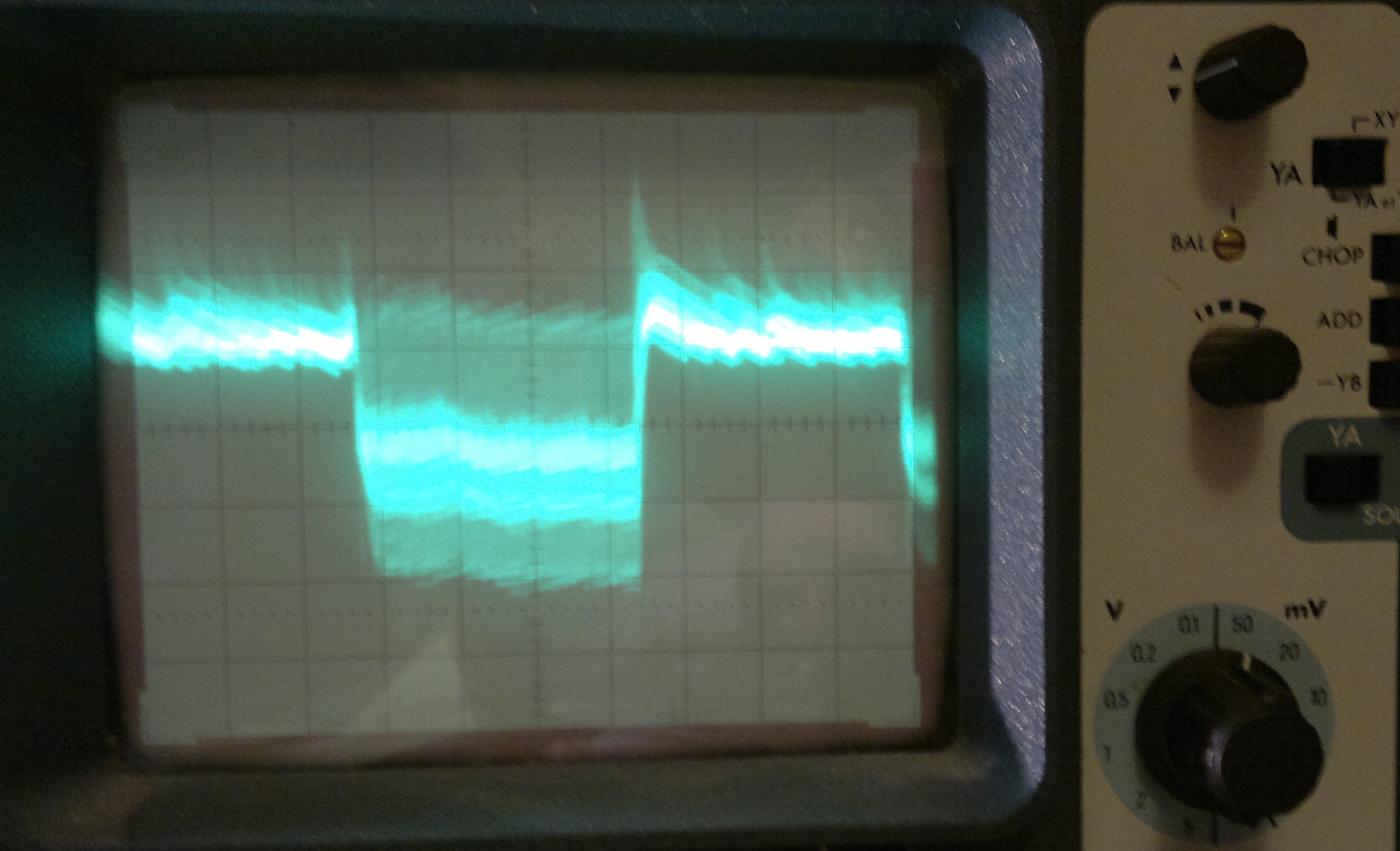
Last test was a measure of converter voltage response (12V side) to a step change in load from 0 to 4A.
Conclusions
I’m happy with achieved results. I wasn’t sure that such circuit will work correctly at higher power. I spend quite a while on experimenting with current measurement circuit but I’ve enjoyed it since rarely one has a opportunity to design some single transistor amplifiers. I’m still planing to test the idea with current probe design. I think I underestimated challenges associated with conducting high currents (20A) trough PCB. I foolishly made thermal isolation to simplify soldering only to then be forced flood them with solder to increase conductivity.
I believe that building such circuit is an easy way to begin experiments with digital voltage converters. Nothing limits the design to be used only as a unidirectional converter but digitally controlled. Despite not having very good regulation this converter is very good in fast current limiting.
In general such converter is capable of simplifying and isolating
the behaviour of real battery from power supply bus. This in turn
allows for connecting collection of different batteries to one low
power decentralized power line. This project is actually a second
part in strive to create a circuit which allows to create this
universal battery building block. This design
steams from one of my previously
described projects
and is a second step in achieving this
goal.