 Aleksa
The origins of this project lie in [bunnie & xobs'] excellent Novena project, which came about around the time I first became interested in hardware. The Novena had an FPGA co-processor tightly coupled to its CPU, which was used alongside a high speed ADC and a front-end (housed INSIDE a probe!) to make an oscilloscope module. This, alongside much aspirational viewing of [Dave Jones'] oscilloscope reviews and tear-downs, got me thinking about designing an oscilloscope myself.
Software Defined?
After bouncing some ideas off of my friends at university, I became convinced it would be possible to transfer every sample from the ADC to the user's computer in real time, with all the triggering and processing being done by the CPU. This would offer huge advantages compared to regular benchtop scopes! Your sample memory would only be limited by the amount of RAM on your computer, as opposed to the piddly 24 Mpts on scopes such as the ever-popular Rigol ds1054z. Waveform update rate could exceed the 1 million waveforms per second offered by Keysight's InfiniiVision series since processing is done on a modern multi-core CPU, unrestrained by BOM cost limitations on FPGAs or by the fixed nature of ASICs. Speaking of BOM cost, by not having to pay for any real processing, memory, display or power supply, this design can be made competitively to other low cost scopes. This savings also allows for a more capable front end, allowing you to get the most of the 1Gs/s ADC by offering 100 MHZ bandwidth on four channels, 200 MHz on two channels, and 350 MHz on a single channel.
Block Diagram
Here was my initial sketch of the design in March 2018. Sorry for the poor resolution, I knew the photo existed somewhere, but could only find a thumbnail file!
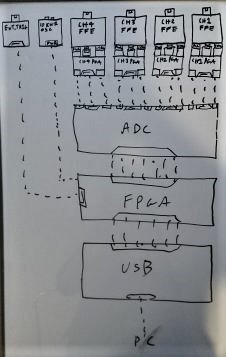
You can see the influence from the Novena oscilloscope module in planning to use all those SATA connectors and in the choice of PGA. The idea was to make the whole system modular, so that each part of the scope could be tested individually. From left to right at the top, we have an external trigger, 10KHz probe compensation, and a module for each channel labeled FFE, for Front of Front End. These modules would hold the input buffer for the next module down the line, the Programmable Gain Amplifier (PGA). This would drive the ADC inputs, and the ADC would connect to the FPGA. The FPGA would handle the external trigger, probe compensation, and convert the ADC's output into something the USB interface could understand. Finally, the USB interface would send all the data to the user's computer.
At the time, there were USB 3 Gen 1 (5 Gbps) interface ICs available and the faster Gen 2 ICs were promised to be in the works. So a Gen 1 chip was chosen with the plan to migrate to Gen 2 when the ICs became available. The parts linked were the ones chosen at the time, so stay tuned for the individual posts for each of the blocks above! Except the external trigger, I dropped that almost right after making this block diagram.
Discussions
Become a Hackaday.io Member
Create an account to leave a comment. Already have an account? Log In.