 Aleksa
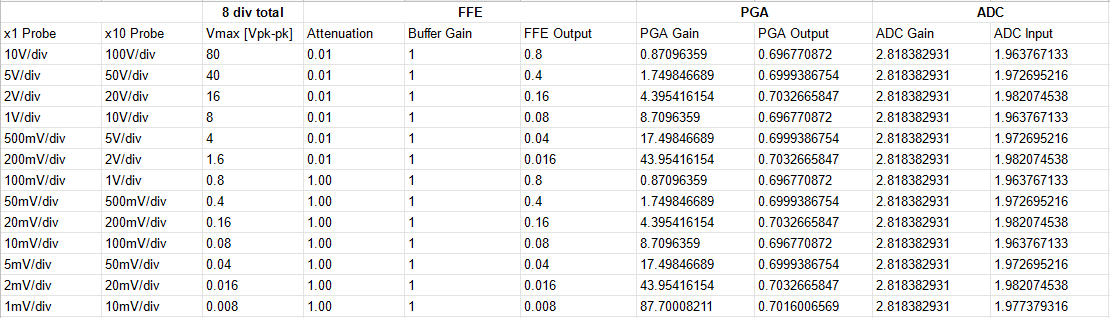
At this point, there was one big issue with the front end. The attenuators could not be switched in without causing the whole circuit to oscillate! This issue was compounded by the maximum 0.7 V output of the PGA as well as the massive cost of the design (three relays and an unobtainium opamp don't come cheap). Since I already had to use digital gain to boost the output of the PGA, I decided to remove the opamp gain stage present in the current front of front end (FFE) board and replace it with a unity gain (x1) buffer. Using a unity gain buffer would allow me to remove one of the attenuators, as it would not need to scale the input voltage just to gain it up anyway. I would also need to use an active level shifting circuit instead of the resistive divider to avoid losing half the signal shifting it up to a DC level of 2.5V. Below is the spreadsheet I used to plan out the attenuation and gain needed for all the voltage division settings.
Let's take a look at the schematic, starting from the input coupling and attenuation block. I chose to remove the 50Ω termination relay to lower cost per channel since this wasn't a feature often used or provided on entry level scopes like this one. The move to one attenuator also saved another relay's worth of materials cost, and I replaced the mechanical relay used for the coupling cap with a solid state relay (U2) to further reduce cost. The input coupling cap and its relay were moved from behind the attenuator to in front of it. This maintains consistent input impedance behavior in AC-coupled mode regardless of the attenuator state, as before it would go from infinite resistance at DC to the 1 MΩ impedance of the attenuator when the attenuator was switched on.
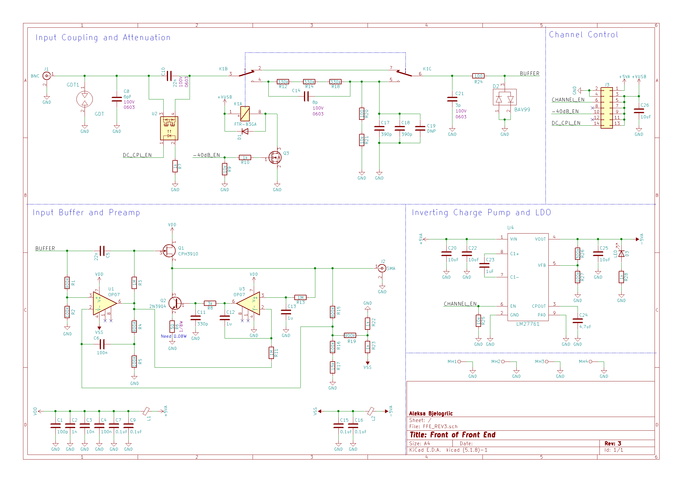
Taking inspiration from the example oscilloscope circuit on page 34 of the LMH6518 datasheet, I used a JFET (Q1) as an AC-coupled input buffer alongside a opamp (U1) to handle the DC portion of the signal while adding the 2.5V offset needed for the PGA input. A JFET was a great choice for a front end buffer since they have very high input impedance and contribute very little noise to the signal. I used a clever circuit from page 34 of Jim Williams' AN47 application note to automatically bias the JFET at IDSS. This point is defined as the current at which the voltage between the gate and source is zero, resulting in a gain of exactly one - great news for our buffer! The circuit works by having the opamp (U3) adjust the current through the JFET using the BJT (Q2) until the filtered DC voltage at the output is equal to the DC component of the input (generated by U1) which by the definition above results in IDSS!
Hopefully this mashup of two interesting circuits makes for a working front end! Join me in the next project log where I go through the testing and results for this board and talk about the next steps I took to perfect this design.
Thanks for giving this post a read, and feel free to write a comment if anything was unclear or explained poorly, so I can edit and improve the post to make things clearer!
Discussions
Become a Hackaday.io Member
Create an account to leave a comment. Already have an account? Log In.