 Aleksa
It's been a while since I posted one of these! I've got a few days before another board comes in so I figured I'd post a log before I disappear into my lab once again. Hardware-wise, we left off after the main board was finished. This board required a third-party FPGA module, which had a beefy 100k logic element Artix-7 part as the star of the show, costarring two x16 DDR3 memory chips.
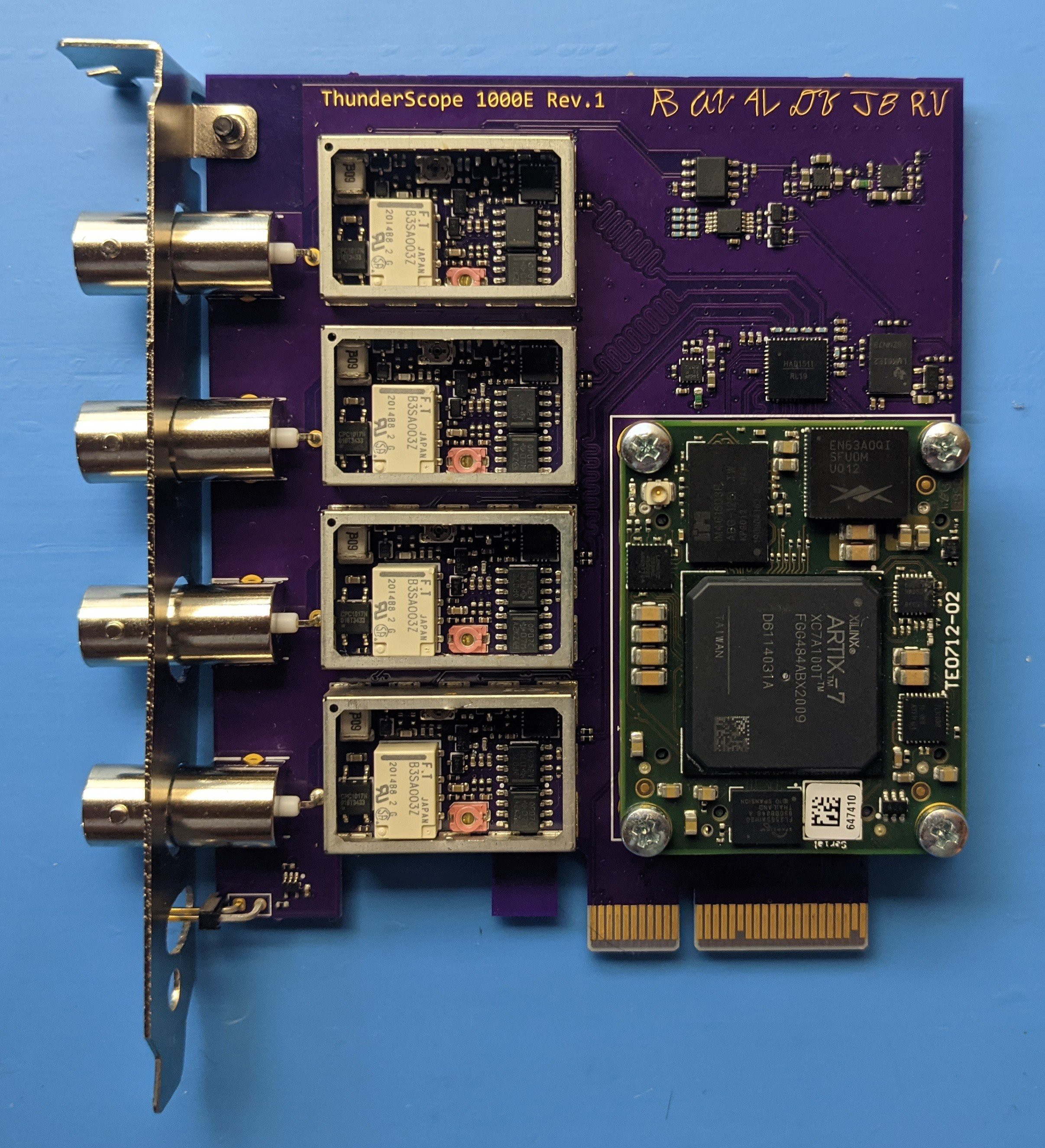
But wouldn't it look better if it was all purple? The next step was to build my own FPGA module, tailored specifically to this project.
First, I did a few optimizations to the FPGA design to make it fit into the 35k logic part. Most of these involved digging around in the PCIe core, changing whatever values I could and seeing if it lowered the logic count without affecting performance.
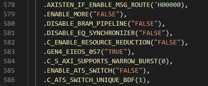
Could it be that easy? Unfortunately not, enabling "resource reduction" only saved a couple hundred LUTs (look-up tables, a finite FPGA resource).
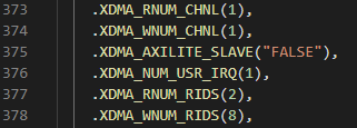
The GUI does not allow you to disable the read DMA channel, so I set it to the minimum number of RIDS I could to try to reduce the logic used by this unused channel. But in the code was an opportunity not just to go to zero RIDs, but to perhaps disable the channel completely! After a very tense compile cycle, it netted a savings of a few thousand LUTs! More importantly, it kept working with the software too (as it never even instantiates the read channel).
Now that the code fit the smaller (in logic count) part, I decided to use the physically smaller CSG325 package part as well to lower costs even further (the CSG325 is about $10 cheaper through distributors than the FGG484). This came with a few challenges! First, the IO banks for the ADC LVDS lanes (which had to be 2.5V to use internal termination) and the other GPIO (all 3.3V) would have to be merged. I resolved this by using external termination resistors on the LVDS lines to allow the whole bank to be powered by 3.3V.
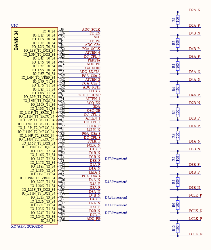
The next challenge was fitting a x32 wide DDR3L interface on this part. This required two IO banks in the same IO column.
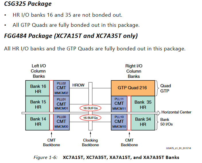
The only two banks that would work were banks 14 and 15, however bank 14 also holds the SPI signals for configuring the part from an external flash memory. There are only five of these signals so it isn't a problem of using too much IO, but again a problem of IO voltage. DDR3L runs at 1.35V and most SPI flash won't run lower than 1.8V, so some sort of level conversion was needed. Luckily enough, someone at Xilinx had thought of this and detailed how to do it in this appnote.
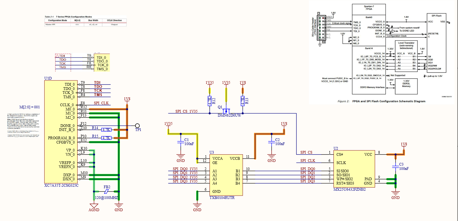
The configuration interface is the one thing you can't reconfigure, got to be careful.
With the schematic sorted out, it was time to layout my first design with a big BGA part and DDR3 memory!
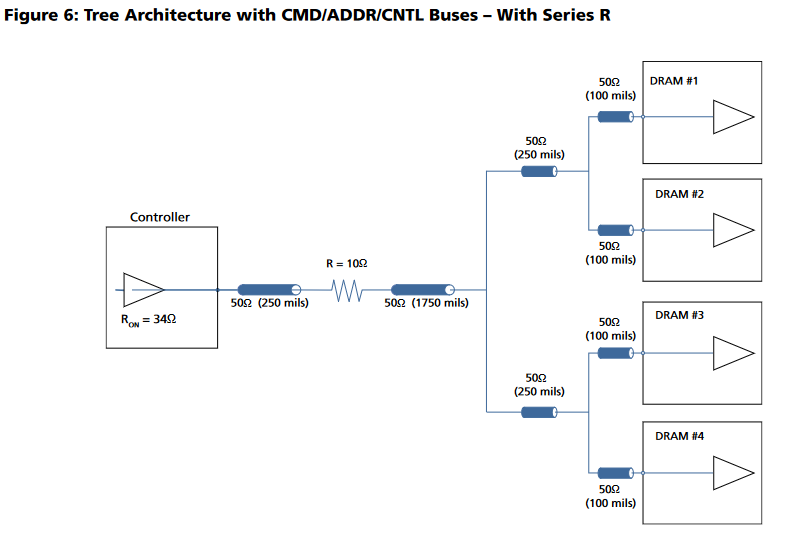
This diagram shows the way I routed the non-data signals (all data signals have on-die termination and don't branch out). Each branch of the tree must have equal lengths as well.
I accomplished this by placing the two DDR3 chips in the same location, one on the top and one on the bottom. I then length matched each trace on both sides (the branches) to a field of vias and brought all the signals out to the FPGA on another layer.
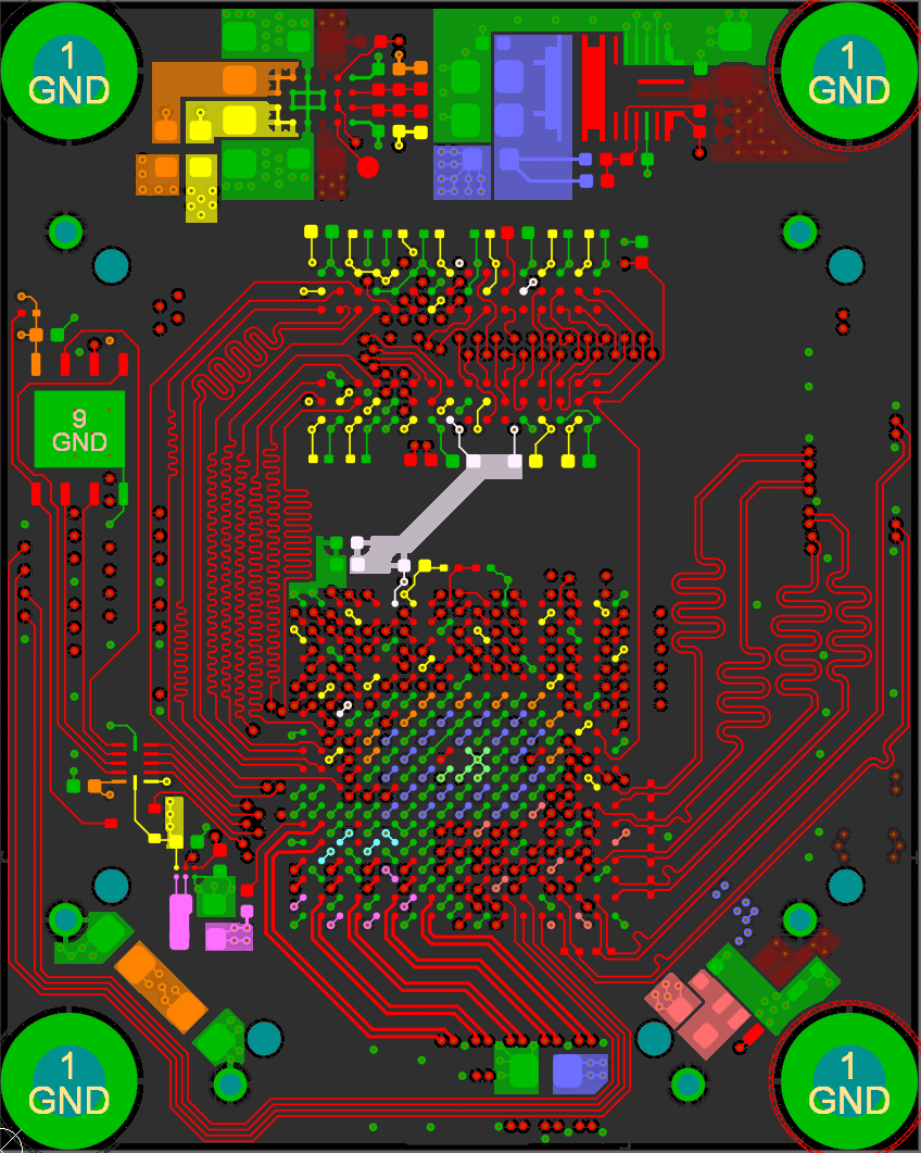
Open the above GIF in another window if it's stopped and you'll see the whole layout. The rest of the data signals just needed some length matching, though it was tough to fit all those signals in to each layer!
 After placing *wayyy* too many 0201s, here it is next to the module its replacing!
 And finally, the purely purple prototype! Follow this project to catch the next mainboard revision, where we will be integrating Thunderbolt in a supremely janky way!
Thanks for giving this post a read, and feel free to write a comment if anything was unclear or explained poorly, so I can edit and improve the post to make things clearer!
Discussions
Become a Hackaday.io Member
Create an account to leave a comment. Already have an account? Log In.
Looks promising, keep it up!!
Are you sure? yes | no