 Max Schnorpfeil
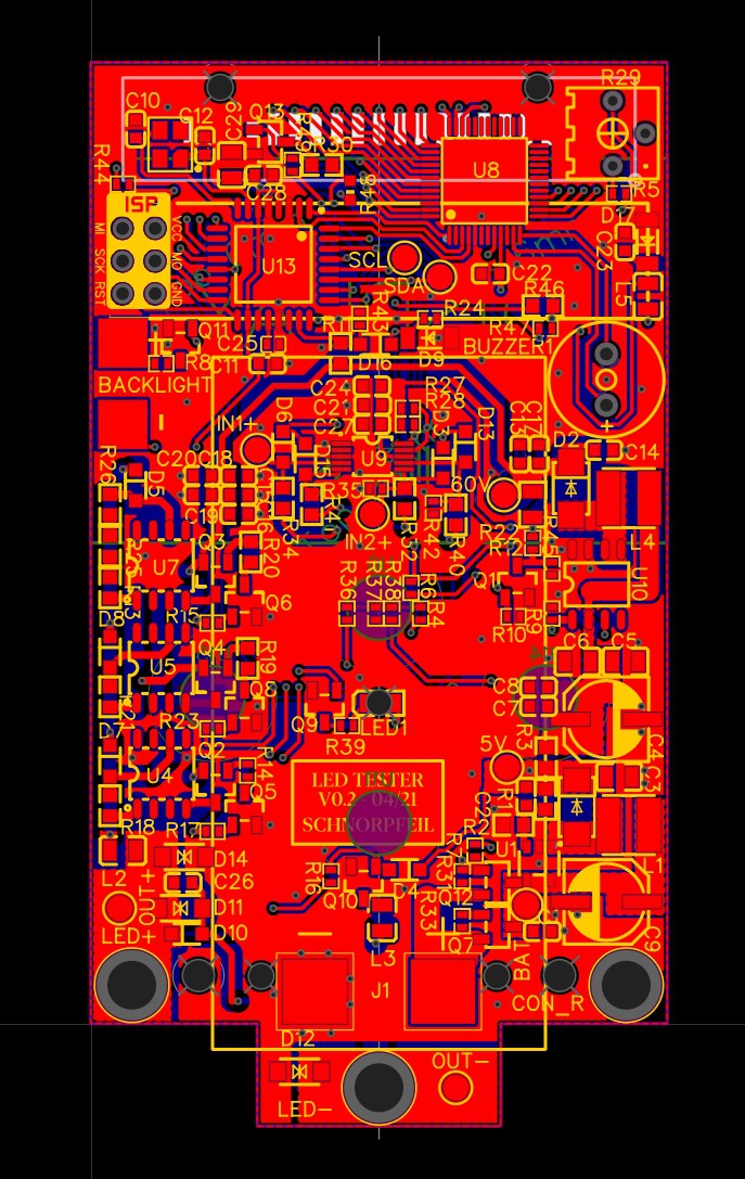
Layout is done using EasyEDA. You can view the files here.
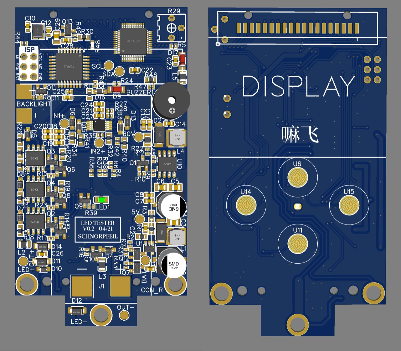
It's a 2-layer board with 1.0mm thickness. Might go for a better 4-layer stackup in a later version for EMI purposes.
More on good stackups can be found in Robert Feranec's videos (like this).
Discussions
Become a Hackaday.io Member
Create an account to leave a comment. Already have an account? Log In.