 Ken Yap
There are 16 locations addressed by the address nybble of the 8-bit code word. We allocate the bottom 8 locations to I/O, and the top 8 locations to scratchpad memory which is used for temporary booleans. Input 0 is special, it's the Result Register. Being able to read back the RR is required for most configurations. Here is the Logisim circuit:
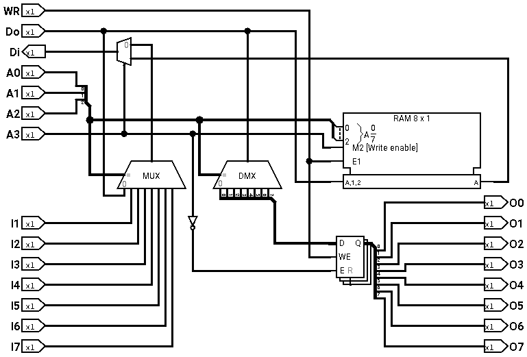
As expected, A3 is used to disambiguate between I/O and scratchpad locations.
A couple of notes: The demultiplexer and output register could be combined in one chip so the 8-bit bus between the two is intrachip. The 2 to 1 selector between the multiplexer and the RAM could be dispensed with if both of them support tristate outputs switched by A3 of course. Both these points highlight that often Logisim doesn't have the parts that exist in the real world, although they can be synthesised by existing gates. Or one could write a Java implementation of a chip, but that is more work. We shall return to this point.
Discussions
Become a Hackaday.io Member
Create an account to leave a comment. Already have an account? Log In.