 Blecky
Here is the traced out SPI/comms configuration for the NXP Explore NFC RasPi board:
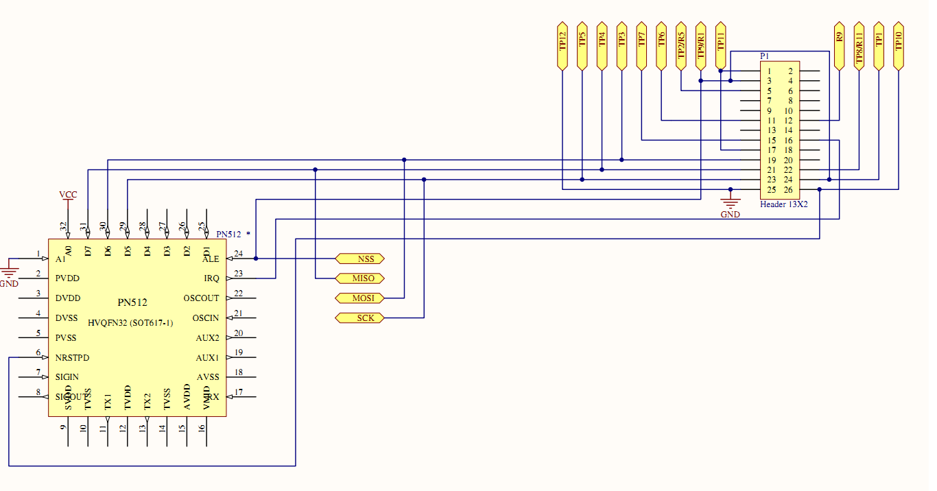
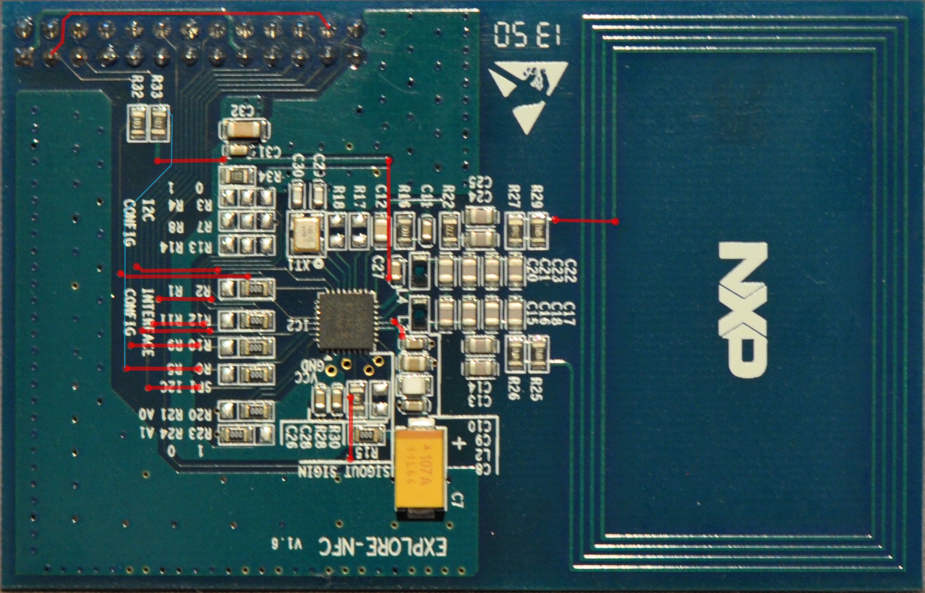
On the board are 0-ohm resistor links to reconfigure as I2C. I have marked where appropriate, the connection pads for these. The header here corresponds to the this image. The TP designations are test points located on the bottom of the board.
When reconfiguring, you will need to move the resistor links. Here is the board layout when configured for SPI:
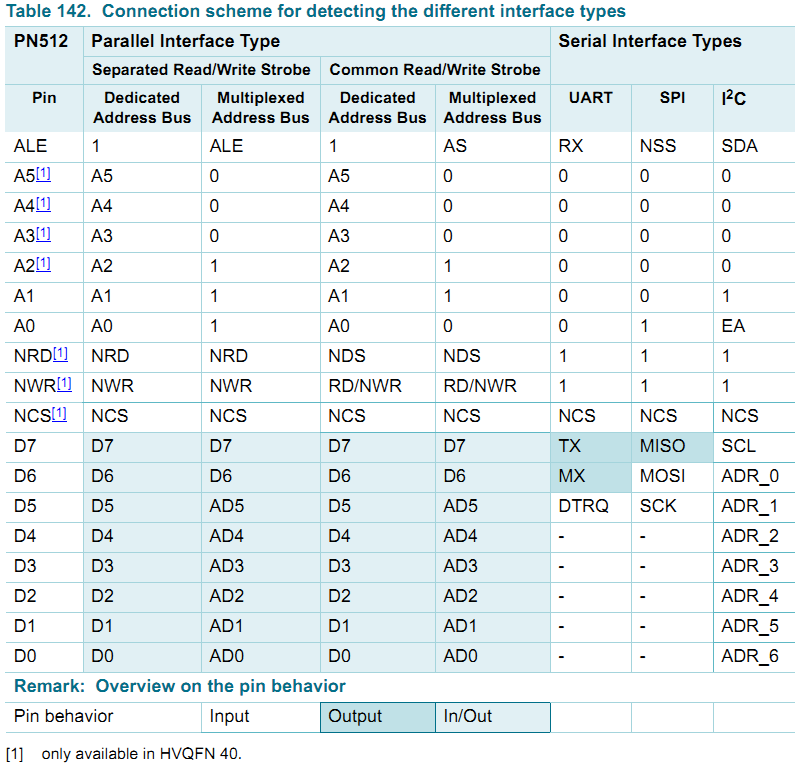
When reconfiguring, be mindful that the PN512 auto detects the serial connection based on the configurations from the table below (taken from the datasheet):
So what was the issue I posted in the previous log. Well notice that pin 3 and pin 24 are connected together. Pin 3 in this instance is used for NSS (!Slave Select) from the SPI comms (as per the software library too). If we are to use I2C for other things (using the default pins on the RasPi for this) we would need to remove pin 3 from this board (pin 5 while connected, doesn't connect to anything except a bare pad. We could remove this too to reduce noise.
Because I will be using an intermediate dev board layered between the NXP board and the RasPi for the prototype circuit, I can just shorten the pins that will be connecting to these points without actually modifying the NXP board.
I am using an extra tall stacking header to perform this sandwiching/connection, so I just have to make the appropriate pins shorter so they do not connect to this board.
All that is left to do then is modify the software to use pin 24 (GPIO 8) for NSS, swapping that with GPIO 0/2 (depending on board rev).
Discussions
Become a Hackaday.io Member
Create an account to leave a comment. Already have an account? Log In.