 agp.cooper
Control Design Logic
Control design logic is a bit of an art.
Yes you can use a Programmable ROM or a PLA but for me, it more fun to use hardware logic.
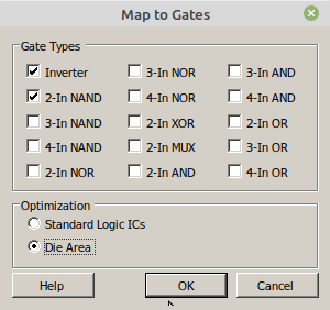
Enter Logic Friday 1
Providing you stay within the limits of "Logic Friday 1", it is quite fun to use.
Create a logic table, solve the "sum-of-products logic expression" (i.e. minimise the logic equations/table) and export a minimised logic gate design.
For large tables Logic Friday 1 can import a spreadsheet CSV file.
For tables larger than what Logic Friday can handle, the underlying logic solver program "Espresso" can be used directly.
Worked Example
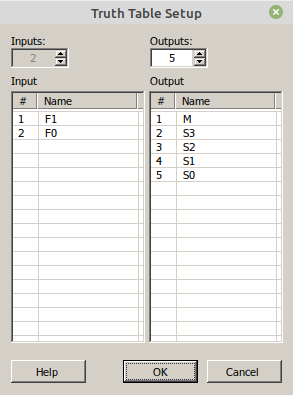
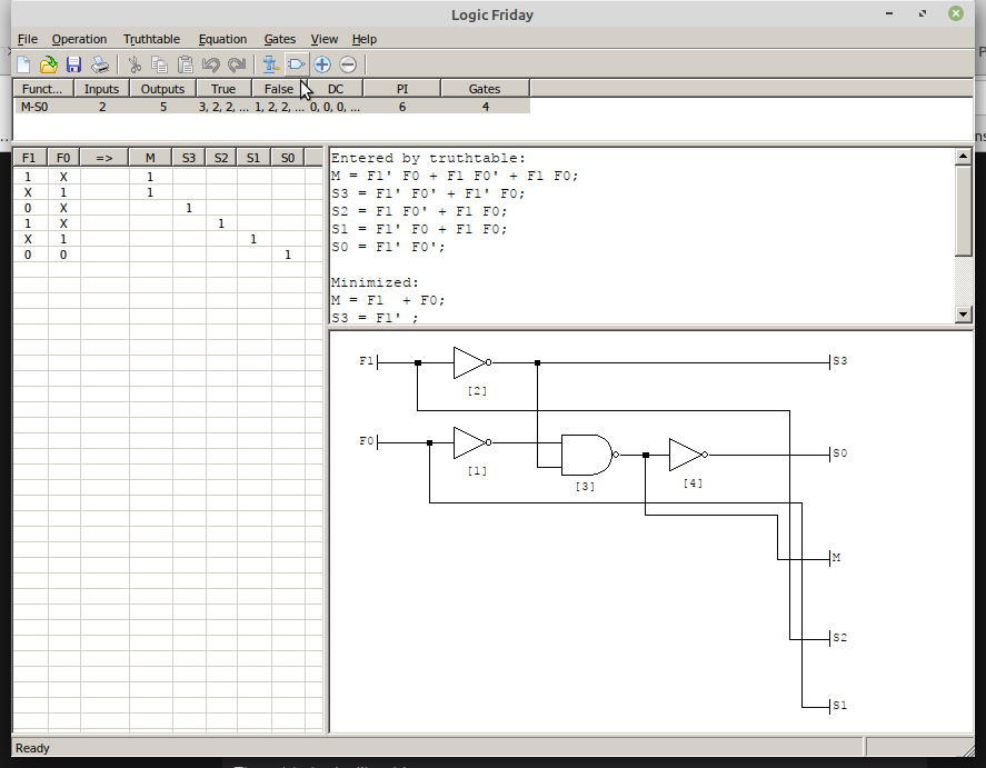
Consider recoding {M,S3,S2,S1,S0} to {F1,F0} for {ADD,LOAD,NAND,XOR}.
The table setup looks like this:
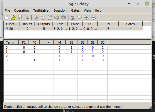
Next populate the table:
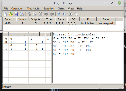
Next close the table and look at the pre-optimised equations:
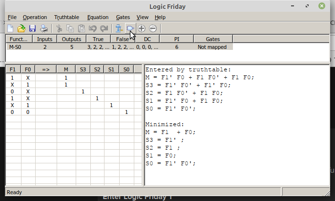
Now hit the "meat grinder" to minimise the equations, that is solve the "sum-of-products logic expressions":
At this point you could use the minimised table to design the logic gates directly say using a AND-OR PLA (Programmable Logic Array).
But for small problems it is easier to use the built in logic gate designer:
And finally:
If you want you can check the design with the built in trace function:
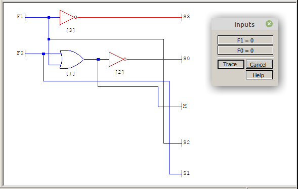
Note: Blue is logic low and red is high high.
If you have not worked it out the last two schematics are functionally the same.
AND-OR PLA
PLA stands for Logic Gate Array and are usually configured as AND/OR logic. However you can also NAND-NAND (active high output) or NAND-AND (active low output) logic.
Here I use a 74HC138 to decode all the logic states (active low) for the Instruction Decoder. As I would prefer active low logic (to suit active low enable on most of the latches) for the outputs, I have used AND gates to decode the logic:
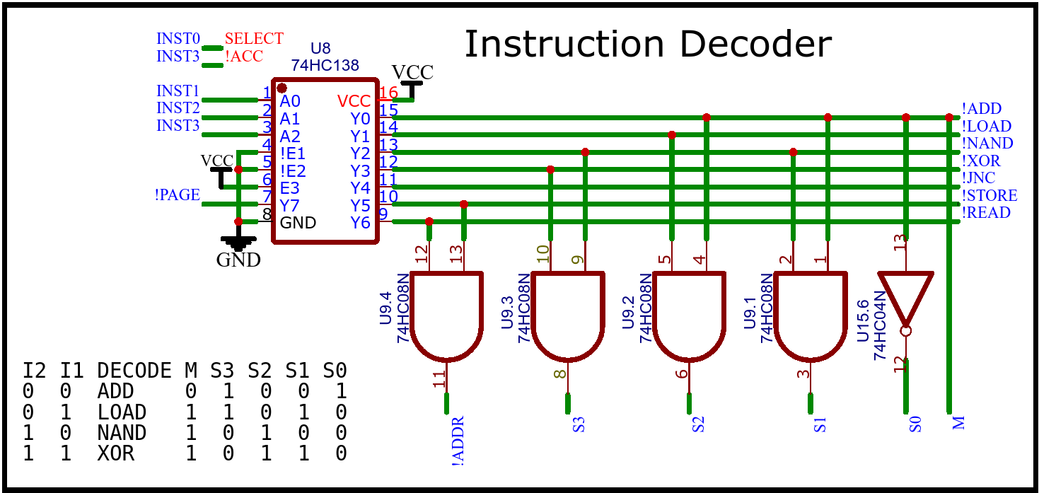
Note: I only decode I1/INST0 and I2/INST2 as I0/INST0 and I3/INST3 were trivial.
The 74HC138 approach can be expanded to suit more complex instruction sets.
Mapping the Jump Logic
The jump logic for CHUMP was not immediately obvious, here is the truth table:
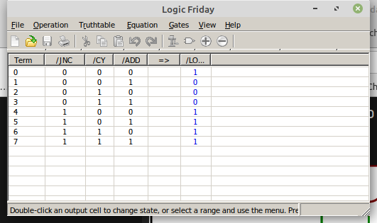
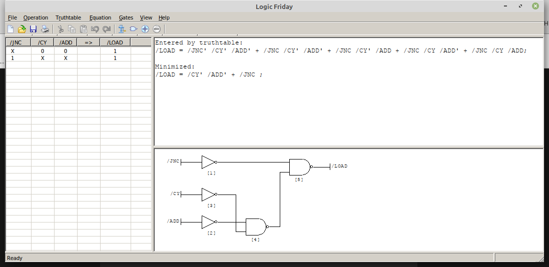
And the result:
Okay, The jump logic is a bit more complicated in that !JNC is only active immediately after an !ADD, otherwise it should be treated as an unconditional jump (!JUMP). This is achieved by delaying !CY and !ADD with a clocked d-latch.
Here is the final schematic:
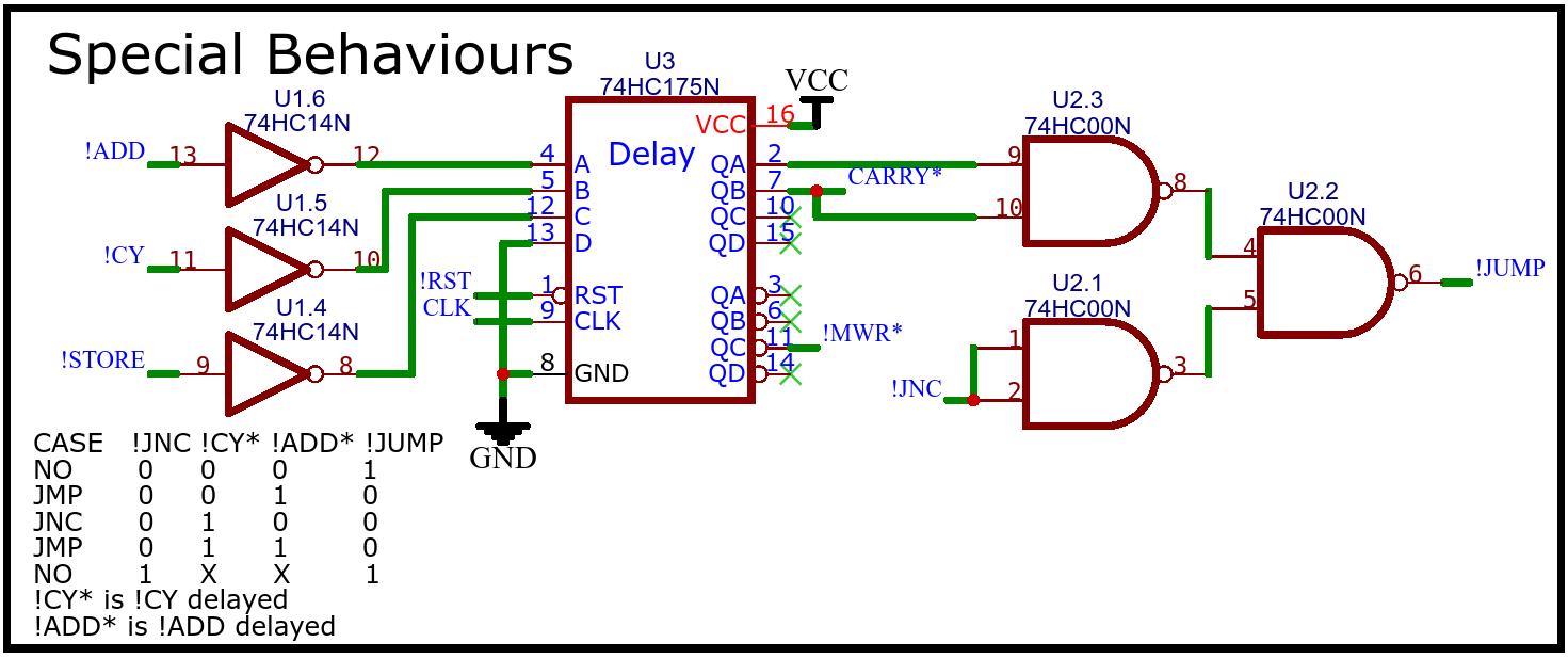
Note: For the delayed memory write (!MWR), the logic is inverted twice so that upon reset the default logic level is high (as the reset (!RST) clears (set logic low) the d-latch).
Hope this has been fun!
AlanX
Discussions
Become a Hackaday.io Member
Create an account to leave a comment. Already have an account? Log In.