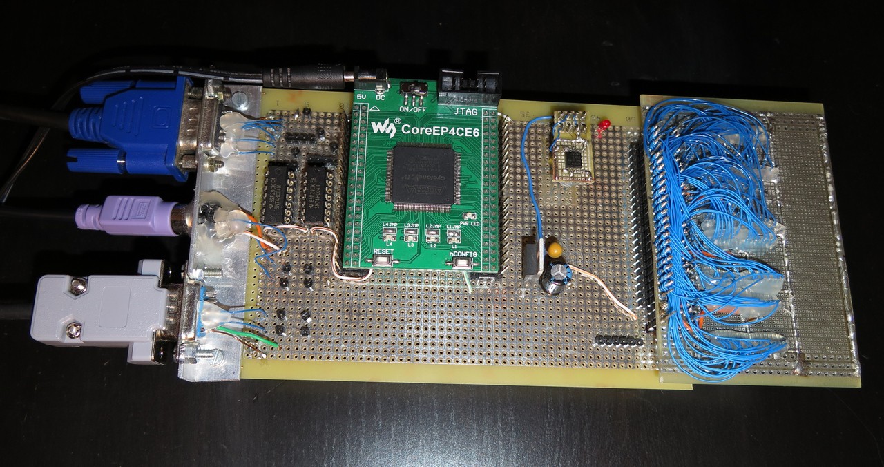
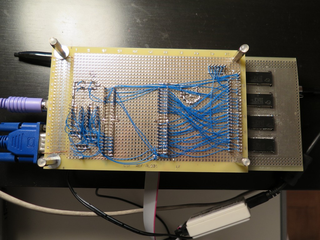
I have built this development board by myself, using wrapping technique, because I couldn’t find any board with 2MB of SRAM arranged in 16bits. I wanted SRAM, instead of DRAM, for the simplicity.
I also have to admit that I like soldering and wrapping. For me, an
electronic project must contain soldering, and otherwise it would not be
fun.
Main components used:
- FPGA : Wave Share Core EP4CE6 breakout board (ALTERA Cyclone IV FPGA with 6000 logic cells)
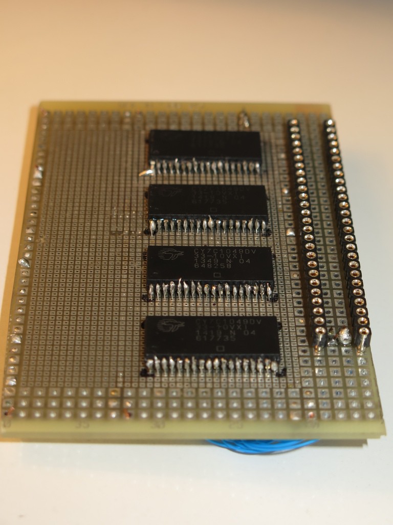
- SRAM : 4 x CY7C1049 (512k x 8 bits)
- FLASH : Micron N25Q128A (16MB)
Wiring table (sorry, awfull scan)
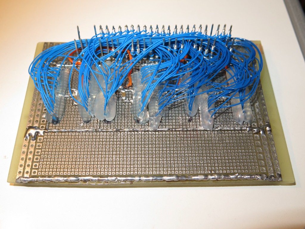
For SRAM chips, I have used SMD. The 30AWG wires are soldered on the SRAM side, and wrapped around the pins on the other side. The wiring of the SRAM board is quite dense, with more than 120 wires.

But making this board is only a very small portion of the project. Most of the complexity of the “hardware” is hidden inside the FPGA, in the Verilog code, described in the following chapters.
 f4hdk
f4hdk


Discussions
Become a Hackaday.io Member
Create an account to leave a comment. Already have an account? Log In.