 Dave Collins
So This week I wanted to do a more in depth look at the ALU unit I have been building up. And since I didn't really get a chance to do a full deep dive post last weekend, This week there are two! In addition I have Partnered with PCBWay on a small power supply for the breadboard CPU which I'll be doing an exclusive build write up, PCB's designed over at CircutDigest. Its not my design but I needed something simple moving forward and I've been wanting to build something like this for a while now. PCBWay has kindly offered to cover the costs of prototyping for that project if ill do a small write up on my experience with their services, so if after you take a look at this why not head on over to my main project page, where you can find the write up on the power supply project. With that sorted, wanted to take some time to talk about the main attraction, the State Machine ALU.
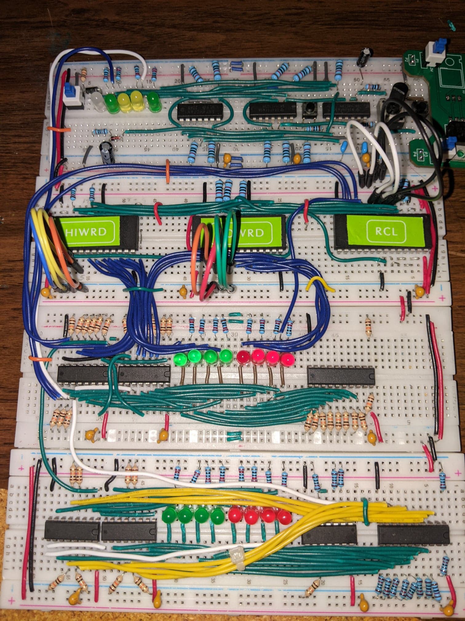
Here it is pictured above. The module with the three EEPROMS is the state machine. The ALU's logic is 100% comprised of 32K eeproms (w27e257 specifically) :
These chips are inexpensive, available as pulls/used, and mostly available from the usual sources such as EBAY / Amazon (I've had good luck so far but your mileage may vary).
Using an EEPROM as a state machine is not new, but in these times finding parts for an actual PLA is getting interesting. In this case EEPROMS fit the bill nicely. Additionally I have a TL866 microchip programmer witch works out of the box at the 12v programming voltage these less desirable chips require.
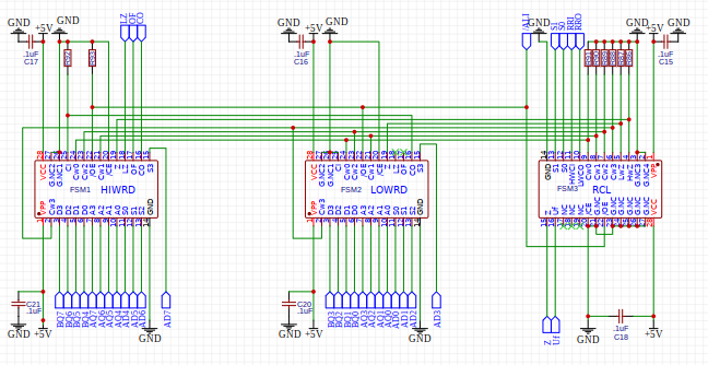
The Schematic for the ALU is fairly simple, I've re-labeled the inputs on the parts in EasyEDA to make the schematics more readable. The first two EEPROMS take care of the actual operations, while the third performs register and flag control. This absolutely could have been further simplified by using a 16 bit EEPROM for more states, but 32k EEPROMS are what I had on hand. When there's a chip shortage you kind of have to work with what you have. You'll note there's still two whole address lines unused on the main logic EEPROMS. Initially this was due to the 12 input limit Logism has for building a truth table, I later expanded it to 13 using some trickery in my tool chain to merge two truth tables together. the remaining two inputs are wasted, for the time being but could not really be efficiently used due to that limitation. That being said, I am planning on switching to Digital Logic simulator but I haven't tested this simulator to determine the limits for truth tables but this looks promising.
Each 4 bit unit is tied directly to the registers outputs before the bus transceiver. Its important to remember the EEPROMS always compare the registers regardless of the state of the clock (unless the EEPROM is placed in cut off by puling /ALI high.) The output writes directly to the input of the accumulator on the falling edge of the clock. This is of course a function of the universal shift registers which make up the accumulator module we've discussed elsewhere.
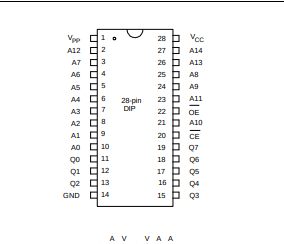
The two 4 bit units are different in a few ways and they all have to do with the arithmetic functions. Looking at the original COS-MOS part, we can see how the original compares to the state machine.
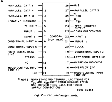
As you can see there are VDD/VSS pins on this and most COS-MOS parts, this was as i understand it (and somebody please correct me if I am wrong), in order to establish a high / low range for the part. The TTL/CMOS ROMS are only 5v but the original parts had a much wider input range. The indicator outputs are all covered under a more simplified single flags made on the main ROMS, and flag update signal made in the register control ROM. Zero is handled by all three ROMS with the two zero operations being checked by a logical AND in the register control, and output if both 4 bit units are actually zero. There is no serial bus connection, as simply the register is external to the EEPROMS. Instead, a more traditional carry in / out functions are used for both the arithmetic, and rotate functions. The clock is on the falling edge and is attached to the accumulator register module. The original part was intended to be connected to the parallel data bus directly. I had considered this initially, however, I came to the conclusion this might cause issues. We can assure the clock can never transition to a register update state at the same time the inputs are changing, if we simply assert both states with registers. Additionally the parallel bus was bi-directional on the original part, this instead uses bus-transceivers on the outputs of both registers. Doing it this way eliminates the need to share the d input and control bus, and eliminates the need for logic to control its function. This slightly increases the amount of time it takes to get data in place to compare, however the whole compare and update can happen with the rising edge changing the control word, and the falling edge updating the register, with an expected read, decode and write cycle of at least 3 clock cycles, the ability to compare two registers in a single clock cycle after being staged could increase program efficiency by a considerable amount. Lastly the conditional input lines define the word position or byte width, in our case we are using modes 1 and 2:
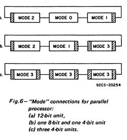
at some point with the two remaining address lines in the ROMS it may be possible to add modes 0 and 3, but for now were working with just 1 and 2. For our purposes MODE 1 is the LOWRD ROM, and MODE 2 is the HIWRD ROM.
MODE 1 AD (source: 1975 RCA COS-MOS Digital Circuits) - "adds the contents of the register to the data on the parallel-data lines and allows any resulting carry to leave on the left serial-data line. The right serial data line is open circuited. The overflow indicator does not change state. The CARRY IN is set to zero. In the case of our state machine, adds the contents of the accumulator to the data-storage. carry in is tied low via an external resistor, there is no serial data line, overflow will output but its open circuited."
In MODE 2 AD (source: 1975 RCA COS-MOS Digital Circuits) "adds the contents of the register to the data on the parallel data lines and the right serial data line. Any overflow sets the overflow indicator. The left serial data line is open circuited. The absence or presence of an overflow is registered. In the state machine, carry in is added to the contents of the accumulator, and the data-storage."
In the case of both Zero, Less than Zero, over flow and carry out are always calculated but flags are only read from the HIWRD and Register Control Logic (RCL) roms. The register control rom outputs a signal indicating when the flags should be updated (all four) this is on every non-rotation operation currently.
the count up control word simply adds a one, and ignores the data-storage. Following the exact same guidelines as the AD control word.
Subtraction is four separate control words, SM, SMZ, SUB, And Count Down:
In MODE 1 SM (source: 1975 RCA COS-MOS Digital Circuits) "same operation as AD except the contents of the register are two's complemented during addition in Mode 1 and Mode 3. In Mode 0 or Mode 2, the contents of the register are one's complemented and added to the data on the tight serial-data line and the parallel-data lines. Overflows occurring in Mode 1 or Mode 0 do not alter the overflow indicator. The presence or absence overflows is registered on the overflow indicator in Mode 2 or Mode 3."
SMZ subtracts the Stored Data from Zero, SUB Subtracts the Data Storage from the Stored Data, Count down subtracts one from the Stored Data. Flags operate identically to the addition operations within the state machine. And all of the subtraction functions follow the same compliment operations as the SM operation.
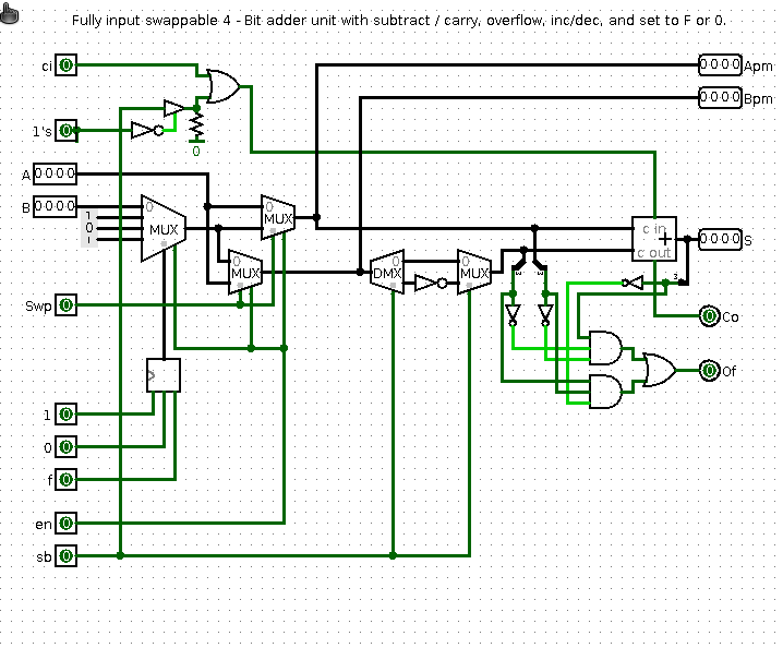
Above is a logical representation of the arithmetic unit. Larger operational functions were used as the goal was to create a truth table, not experiment with combination logic circuits. The basic idea is, this is a select-able 4 bit adder, with fully swap-able inputs, which outputs carry out and overflow. Subtraction is done by inverting the number to be subtracted and then adding it. Additionally you can sub in a constant operator (triggered by logic external to this diagram) for a 1 or 0, which is useful for CU, CD, and SMZ the logic for sending a operator of F ( all 1's) to the adder is also built but I never actually used it in the final design. Because the propagation delay is based solely on the EEPROM and not the internal logic I didn't have to worry about optimizing, since we only care about the resulting truth table.
As you can see the finite state machine has a ton of similarity to the original part, but lacks function and features that are just not possible with EEPROMS. I still consider it a huge hurdle to get a functioning unit at this point, even though it's not pin compatible. The propagation delays of the original part were quite slow, and while an EEPROM ALU is most assuredly not the fastest way to add two numbers, using semi-modern EEPROMS does afford far better than 1970s response time. Its very possible this ALU I've built even on the bread board could run at 3Mhz, and I doubt the industrial control applications that ran on this platform back in the day ever got that fast, its actually hard to tell since even the application notes don't state anything other than response time (in the realm of 100s of nS), and additionally much harder to find devices that were built using these chips. Since its an ALU there's no real concern to making an architecture that is compatible to run existing code, if there is anybody out there who's even got a clue as to what systems this may have been built in to shoot me a line. It would actually be fantastic to see what kinds of things that this chip was used in.
Discussions
Become a Hackaday.io Member
Create an account to leave a comment. Already have an account? Log In.