 Dave Collins
Up till now, the design has been focused on devices solely supporting the ALU. We've talked extensively about the ALU and its inner workings and brushed a bit on the two registers which support it. Moving forward from this mid-point we start to look at parts of the computer that are external to the ALU. Having these systems in place will allow us to test the ALU, as well as support the rest of the CPU and computer system as a whole.
Instruction Register:
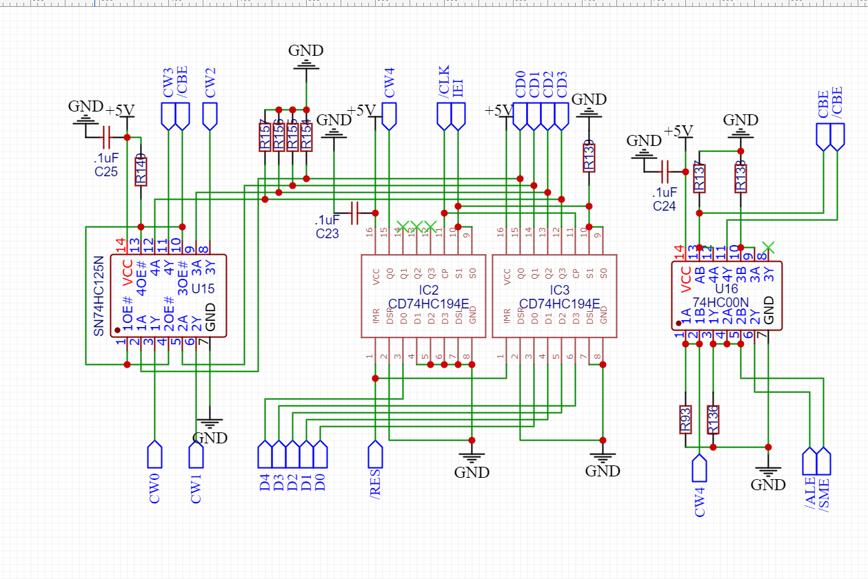
The Instruction register is 5 bits wide, and utilizes 2 74HC194E universal shift registers. I continue to use these registers because they have simple to breadboard inputs, and can be made into a simple parallel load register by simply connecting the the control inputs together. The instruction register outputs are tied to a LED display, as well as the control word inputs on the ALU (and eventually the microcode state machine instruction processor that will handle the other non-math functions.) The inputs are tied to the bus, and can be written to likely using a LOAD function from the instruction processor. An active high pulse from the input decode logic (controlled by the instruction processor, or the ATTINY88 ) enables the Load function on this register. The Most significant bit feeds a inverter tree, which switches the output enable on the ALU or the Instruction processor to determine which will act on the 4 bit instruction bus. This gives us 15 math instructions, and 15 general purpose register and memory functions. There are 3 bits left un-used in the High word register, which allows for some expansion if further instructions are needed we could use this to control other operations, but for now I've decided to leave it to just 30 instructions total. Lastly a 3rd inverter is used to control the instruction cut off, which is used to expose the instruction bus to the command word only during the write cycle(S) of the processor.
Flags / Output Decode Logic:
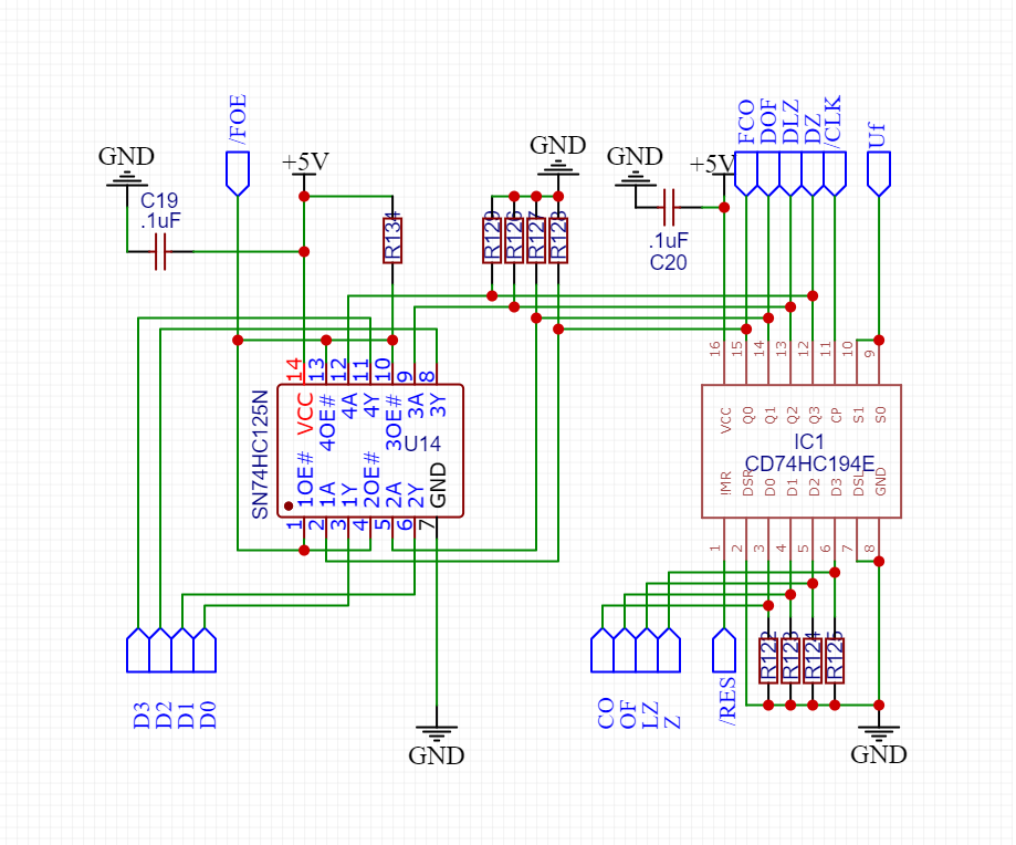
The Flags register records the ALU flags from the last mathematical operation. Its inputs and load instruction come from the register control and high word state machines in the ALU module. Each time a math operation is performed, on the falling edge of the clock, the register will update. The ALU determines weather or not the flags register will update the only time it is Zeroed out would be immediately after a reset; The reset signal of this register will likely be gated at some point in the future to allow it to be zeroed by the CPU, however for now, the programmer will have to clear the Zero state by setting a value in the accumulator using a math operation. The Flags register has it's outputs tied to the bus and can be read out onto the bus to be stored or used elsewhere.
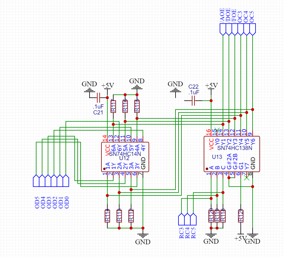
The output decode logic uses a 74HC138N to select which register will output to the bus, an inverter is used to make the selection read out (for the LED's only ) make more sense. In this case the inverter is 100 % simply in place in order to make the Low signal which enables output elsewhere on the computer appear as a high signal (to make the LED's turn on ) when a register is selected. The control bus is a 6 bits (a nibble and a half). 3 lower bits control Register input, and 3 upper bits control Register output. these are connected to the rest of the system via the instruction processor or the attiny88. A third module is made that is basically wired identically to this which decodes the input control logic. As it is basically the same, I didn't feel the need to make a separate entry for taking a deeper look at it.
What is next:
So next up will be testing the ALU, this will be done using the ATTINY88. I opted for building in a modern microcontroller simply as a UART, and to bootstrap the memory. I don't have any grand plans for it beyond simply using it as a UART and a machine language monitor. Using the microcontroller i can simulate the rest of the build in order to find any issues through testing at speed, without actually laying in the parts needed to fully test the CPU. I have had some feedback questioning this decision, and I still think its a good idea because at the end of the day, to build in a UART I would need to manage a clock for timing; and with my adjustable rate design there's no way to do that without a separate clock. Since I have to have a separate clock and chip to enable a serial output I may as well have a programmable one.
Discussions
Become a Hackaday.io Member
Create an account to leave a comment. Already have an account? Log In.