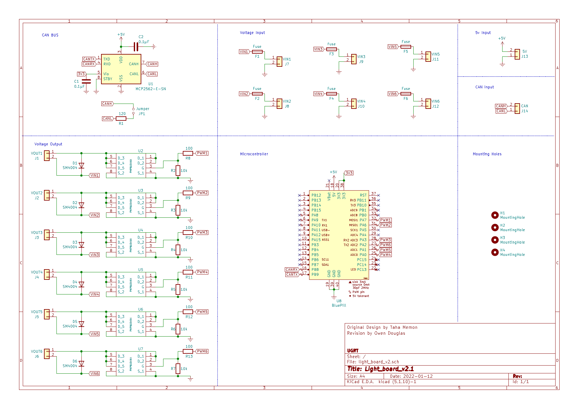
The first step in any PCB design is creating and validating a circuit. This is a vital step, as fabricating a PCB based on a non-functioning circuit is sure to leave you disappointed!

We had validated the 'prototype' of this board with our original rover design, which ran lights from an Arduino outputting PWM signals to control the gate voltage of a power MOSFET. This gate control allows us to take a high-power input from our battery, and control the output voltage so that we can switch on/off and dim the brightness of our LED headlights as needed.
We know this control scheme works from our original rover, but Arduino's do not support CAN Bus natively. Rather than try to interface a CAN > SPI interface with our existing Arduino setup, we decided switching to a microcontroller that does support CAN would be worthwhile. We also chose to update a few other components on the board in order to keep its physical footprint as small as possible so as to fit inside the rover's electrical enclosure.
Many of the components were chosen fairly arbitrarily; passive components for their cost/availability, and the CAN transceiver, connectors, and fuses/fuse holders simply for consistency with other electrical subsystems. There were a few components that needed to be selected carefully though, and these components were chosen as follows:
STM BluePill:
We settled on the popular STM BluePill for several reasons, but mainly because we are already using STM MCUs for several other embedded subsystems, and we have learned that keeping embedded hardware consistent saves a lot of headaches from sourcing and integrating random open source drivers :). It is also small, supports CAN natively, it has ample PWM outputs, and was cheap and widely available before the chip shortage, so hopefully that doesn't last forever!
Shoutout to yet-another-average-joe on GitHub, who has developed some really nice KiCAD footprints for the BluePill. It is important to use a symbol that matches the exact hardware you will use in any design. This seems obvious; however, we accidentally wired up the symbol for the STMF103 microcontroller itself, rather than the development board first. It can be confusing because although the BluePill houses this MCU chip, the pins on the dev board are not a 1:1 representation of the pins on the IC.
Nexperia MOSFET:
We needed a MOSFET that could drive our LED headlights, but also wanted to build in some tolerance so that we could safely drive higher current loads in the future. Another important consideration was that since this circuit is controlled by a 3.3v GPIO output, we require what's called a 'Logic FET', meaning one whose gate can be driven by 3.3v. There are some drawbacks to these type of FETs, mainly higher Rds values, which basically equates to how much heat they produce. For our application we won't be driving these FETs to their limit, and the benefit to using logic FETs is that a GPIO output can be used to drive the gate without adding extra ICs to the circuit such as a gate driver.
With these considerations in mind we settled on the Neperia PMPB10XNX, a logic FET with a drive voltage between 1.5-4.5v, and a max Rds ON of 13mOhm @ 9.5A. We won't need anywhere near 9.5A, in fact there are other design aspects that will limit us to driving a maximum of 3A for each light. This limit comes from the JST XH connectors we have chosen. This board needs to be small more than it needs to be capable of driving high current loads, and since the headlights we currently have only actually draw around 1A, 3A is plenty of headroom and 9.5A is honestly a bit ridiculous anyway! We could always remove the JST connectors from a channel if we needed to drive more than 3A; however, in that case, the 2mm trace width on the PCB becomes the next limiting factor, allowing us to drive a maximum of just under 4A.
Again, this is just a hypothetical discussion to illustrate the limits of our design, but it is important to think about these things before anything is fabricated to ensure the functional requirements of the design have been met. We easily could have used a different MOSFET with a smaller drive current, but this one is cheap, available, and incredibly small for its capabilities, which will help us reach our minimized physical footprint criteria. Also, it has a relatively small Rds value compared to alternatives so it should run fairly cool, especially if we are driving under 20% of its maximum drain current.
 UGRT
UGRT
Discussions
Become a Hackaday.io Member
Create an account to leave a comment. Already have an account? Log In.