 kelvinA
I think, other than the MCU, everything else connects to the PCB via some kind of pad array (a row of pins / pads). Thus, I finally tackled the ESP32 component. This also affected the components I've already made too.
This ordeal seemed more tedious than it really could be in this modern age of 2023, and so I've been imagining what I woud've done if I was making ECAD software (which I might need to look into further if the #SecSavr Suspense [gd0105] / #SecSavr Soapavr [gd0146] can actually fabricate PCBs). Why can't we snip bits of the PDF diagram into some kind of OCR? I've only seen black + white diagrams, so it sounds straightforward (though I know that's usually never the case).
I'd like to mention that part of the reason I actually got through all of this is because of this Aural Scan sound generator I found. It sounds like cinematic background music of a personal technology lab (depending on the preset).
Symbol Formatting
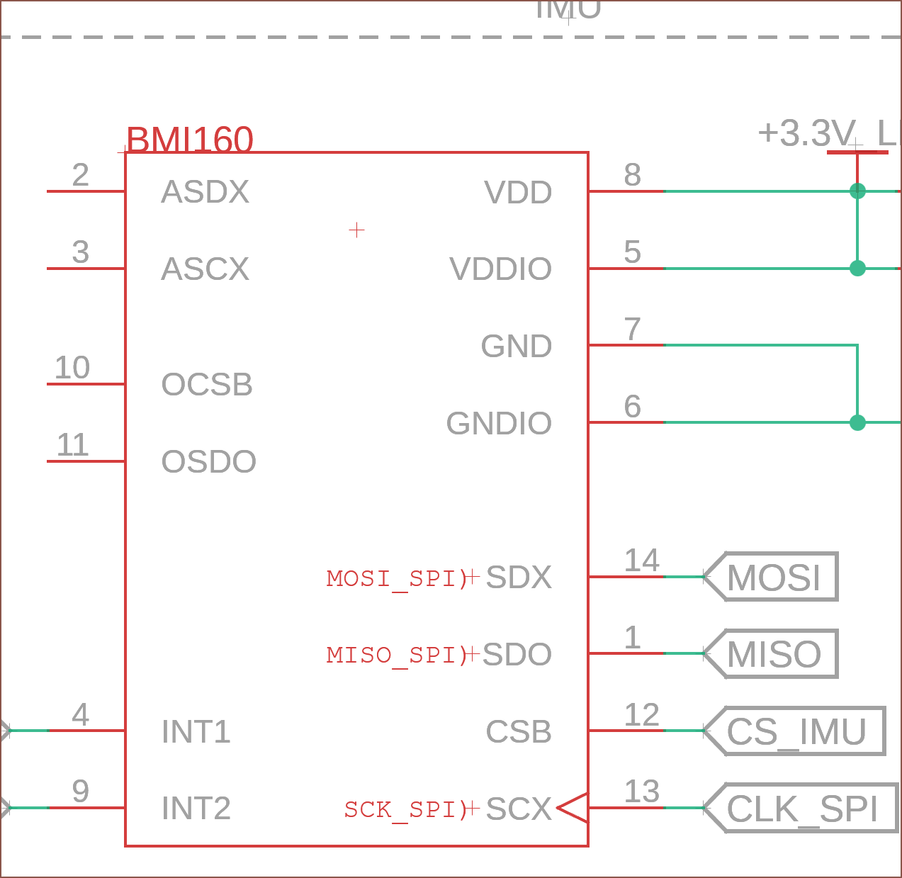
Almost immediately, I thought it was going to be excessive listing every single feature each pin does. Even when I did that for the BMI160, I just used the datasheet anyway.
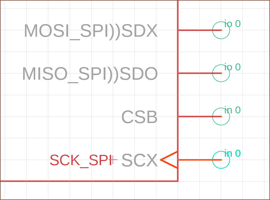
The first thing I did was try only putting the pin function I'm actually going to use in the pin name. Then I got the idea to actually take it out of the pin name entirely and instead make it a bit of text.
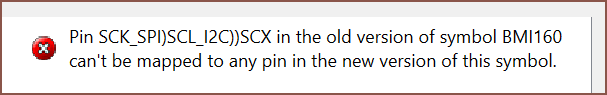
It was a good idea too, since it seems that changing actual pin names could spell trouble.
I decided to change the font of the text to "fixed" instead of "porportional" as the font was thinner and it allows multiple pin definitions to still line up correctly.
I then discovered thad adding '!' puts a line above the text in the pin name (and another stops it). Thus, I've changed all the nPIN_NAME's into !PIN_NAME.
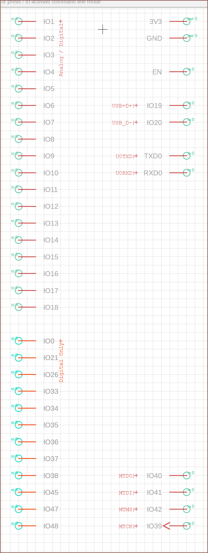
At the moment, there's not much I could really group the GPIO pins into, so I just split them into Analog/Digital and Digital Only. This does make the symbol rather tall, but it's still tidy and compliant with the other symbols.
3D Model
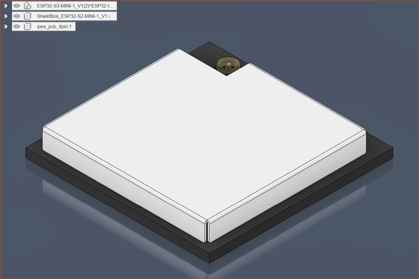
It turns out that there was a 3D model of the other version of the MINI linked in the doc PDF, so I downloaded it and edited it to bring it closer to the MINI-1U. In the PDF, it said that the connector had a diameter of 1.4mm but I could only find models of 2mm ones, so I've scaled it down to 0.7.
Footprint
Certainly the most tedious part of this entire operation.
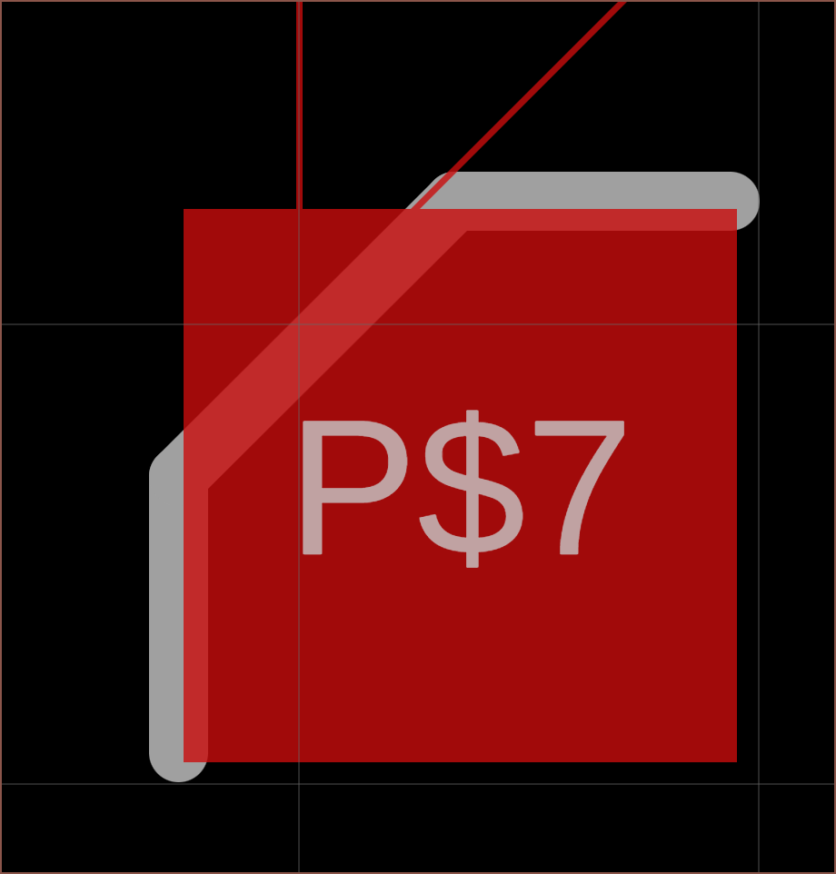
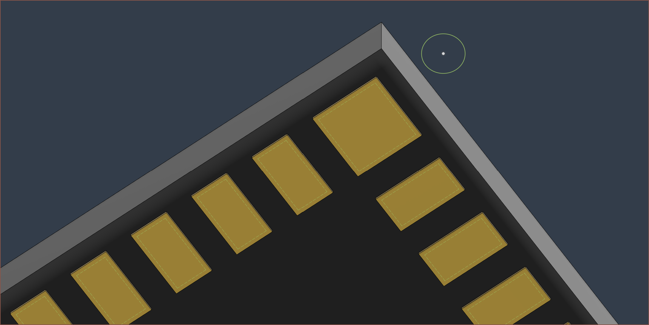
I can't figure out a way to get the chamfer for this pad. Hopefully, a fully square pad is fine.
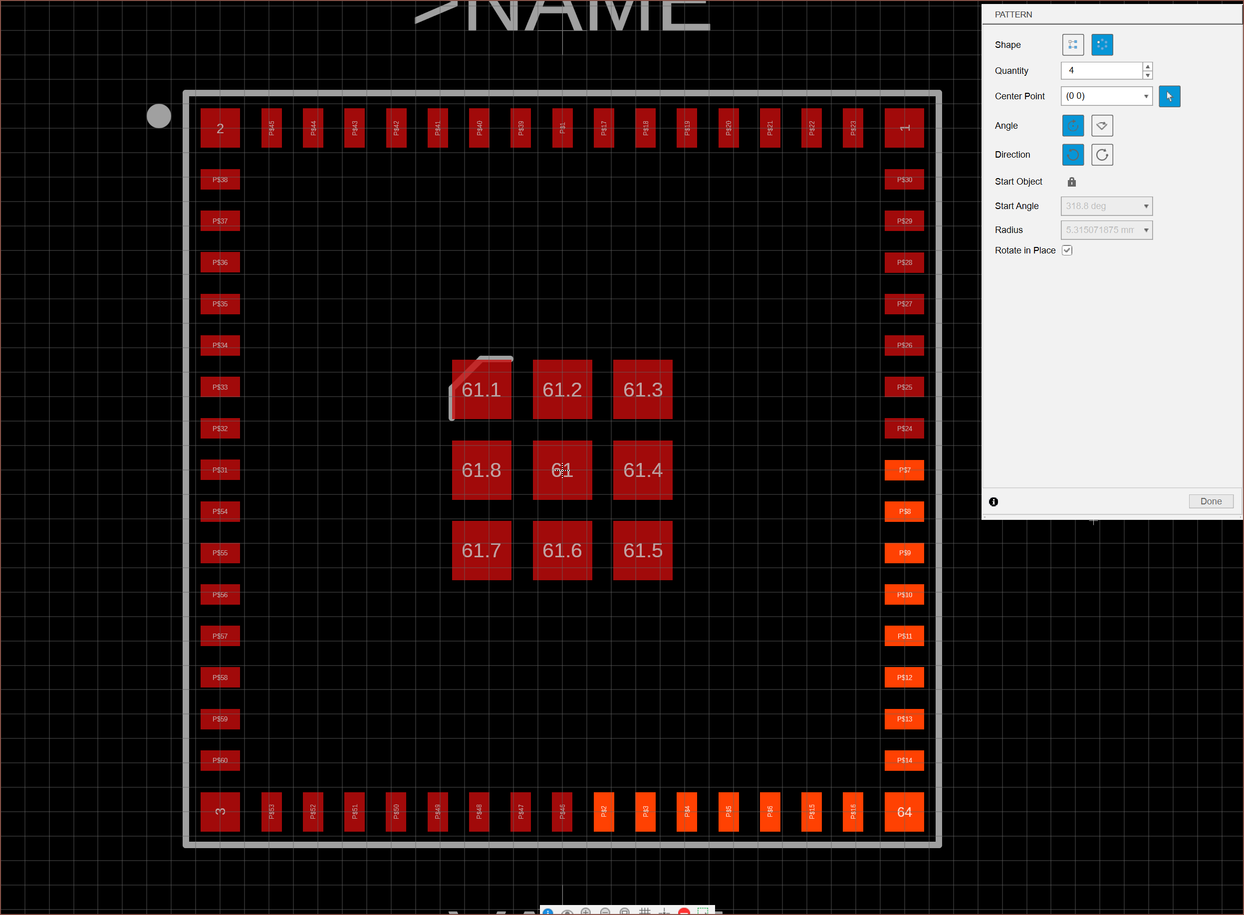
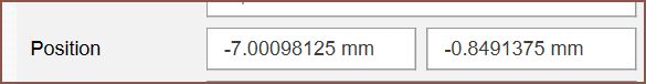
After manually calculating where the first couple of edge pins were supposed to go, I thought I could just create an upwards stack of 8 pads, rotate it around Pin 64, then rotate all of them around (0, 0). The first step worked fine, but the second step brought rounding errors:
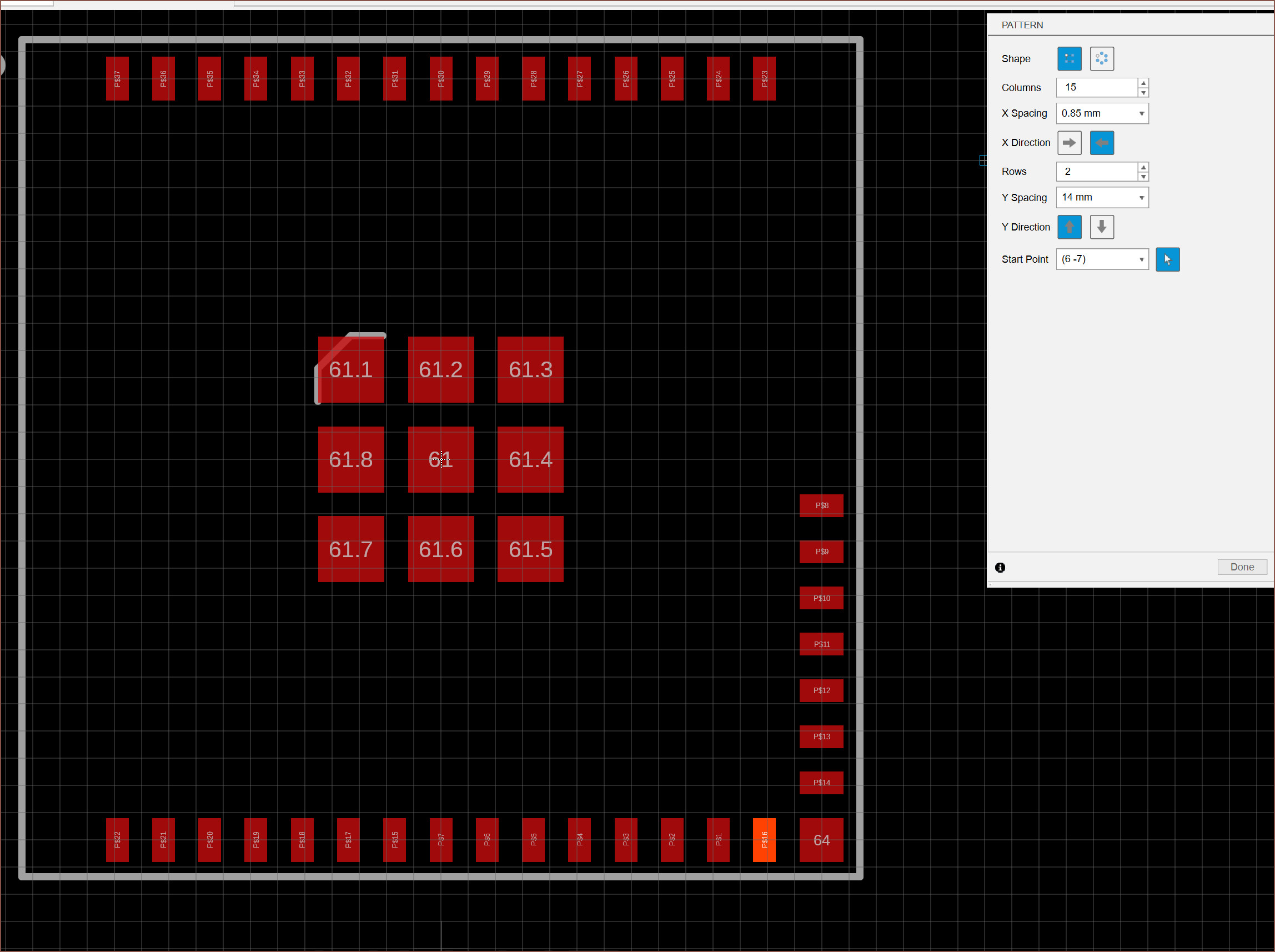
Instead, I used a linear pattern for horizontal and then vertical pins. I also used a linear pattern for the corner squares.
After that, I found out that I could right click the footprint and select "Create New 3D Model" to bring this up:
I still needed to save it before I could drag in the 3D model I made earlier.
It looks like everything lines up fine:
When I was linking the symbol to the footprint, I found out that I missed IO46 and added it into the symbol.
In the schematic
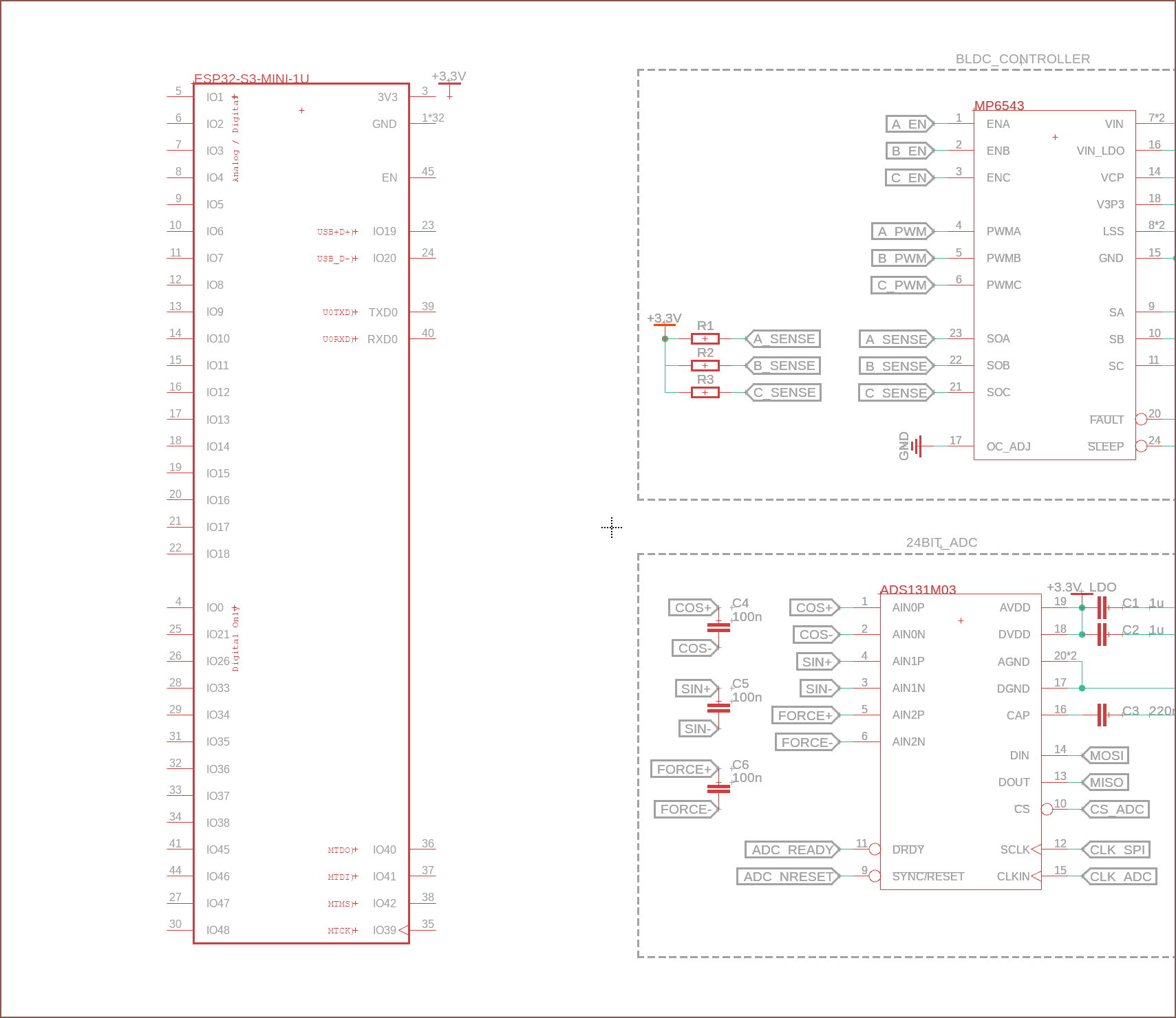
This is what it looks like in the schematic, so I think it's not a bad idea to have all the GPIO pins on one side. I guess this is the small benefit you get from having to make every component, though I am starting to think that this is nullifying the potential speed gains I could've had over doing all this in EasyEDA.
Discussions
Become a Hackaday.io Member
Create an account to leave a comment. Already have an account? Log In.