 kelvinA
So I've spent... oh it's 22:20 now and I started at 1pm... wow it's been over 9 hours?
At this very moment, I've created the symbol and 3D CAD for the AAT101:
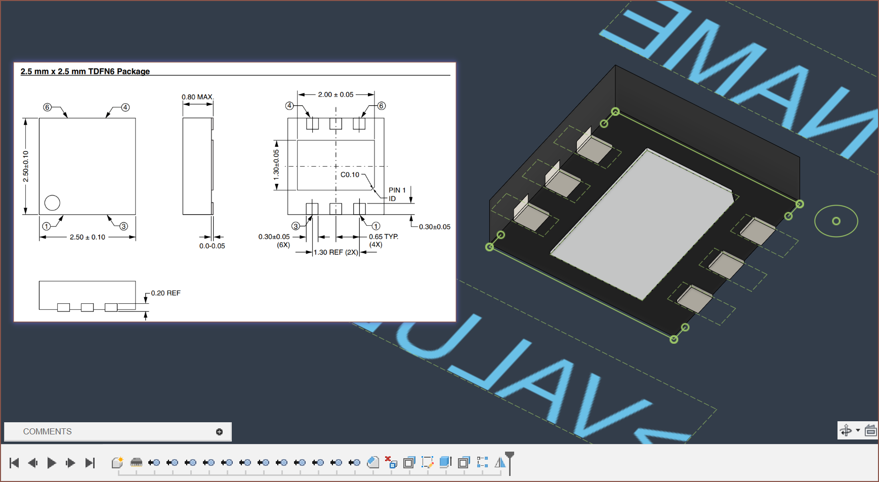
There's a Fusion360 bug where the pads won't generate correctly if the height and width are the same, such as this one. It'll be nice if there was some option to toggle rectangular pads like you can for the footprint.
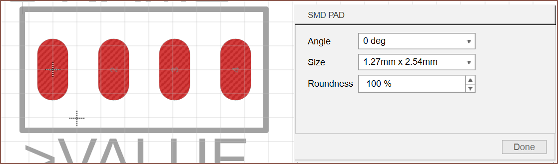
I've now also created the pad for the load cell. I'll assume that a 2.54mm pitch is easy enough to work with, though I may need to shrink down if it's too large on the PCB.
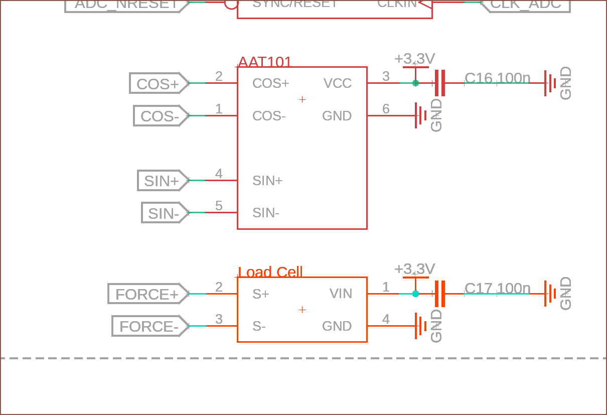
Since the AAT101 is literally just a wheatstone yet specifies a 100nF capacitor in the BOM, I'm going to do the same for the load cell.
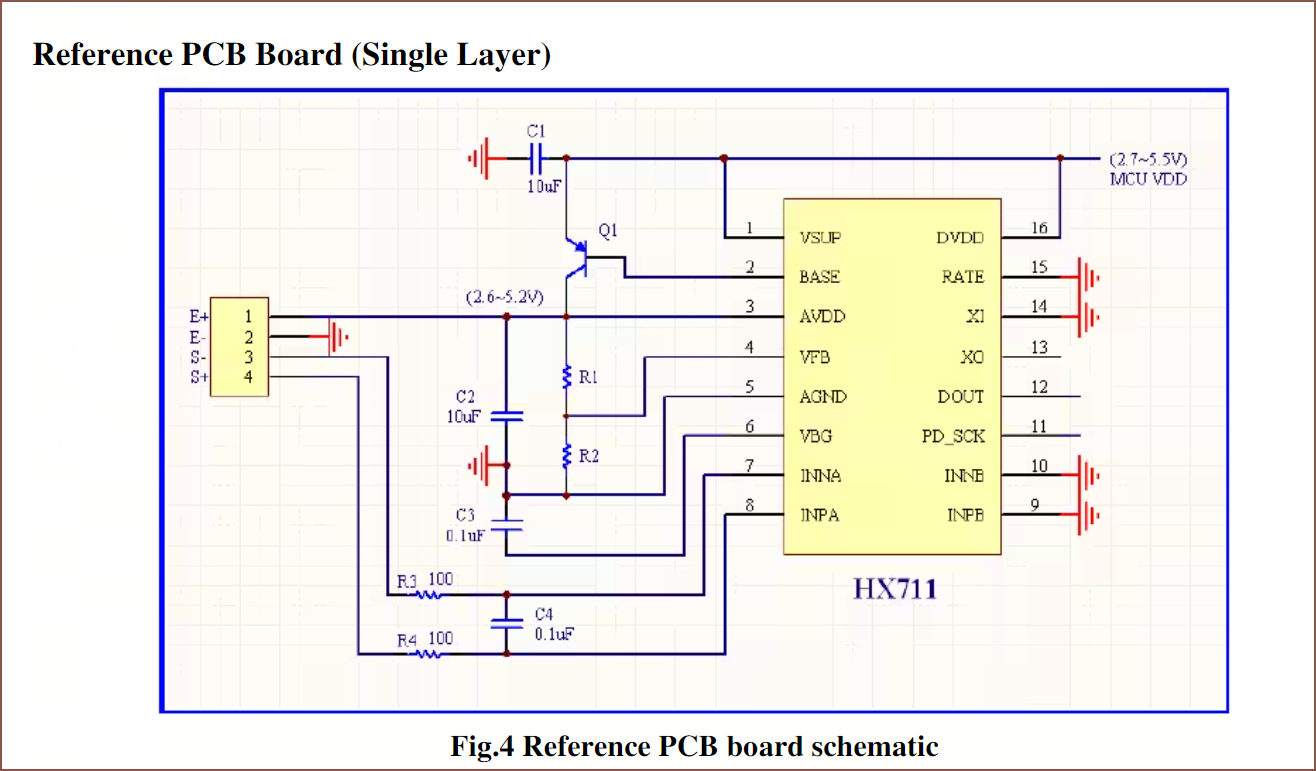
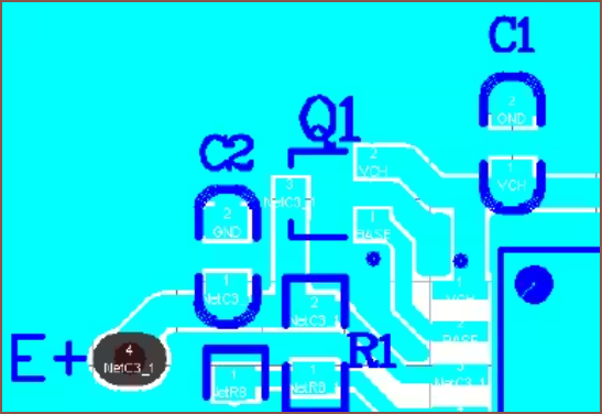
In this reference PCB I found, the bypass is even larger, but it's also connected to a chip so it's hard to tell if it's required for the load cell or not. It's location on the PCB (C2 in comparison to C1) suggests it is, though. Well as long as the pad is there, I can change it later on.
In other news, I've...
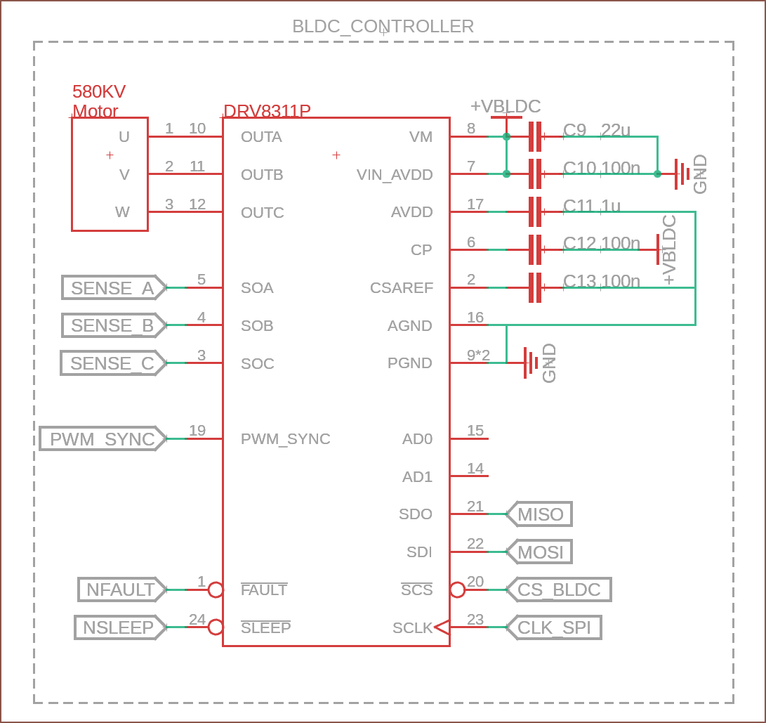
...wired up the BLDC:
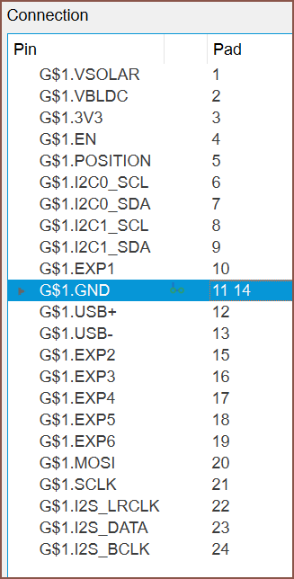
...fit all the pins on the MINI-1U and removed the 595, as well as set up the power and enable pin (as per datasheet recommendations):
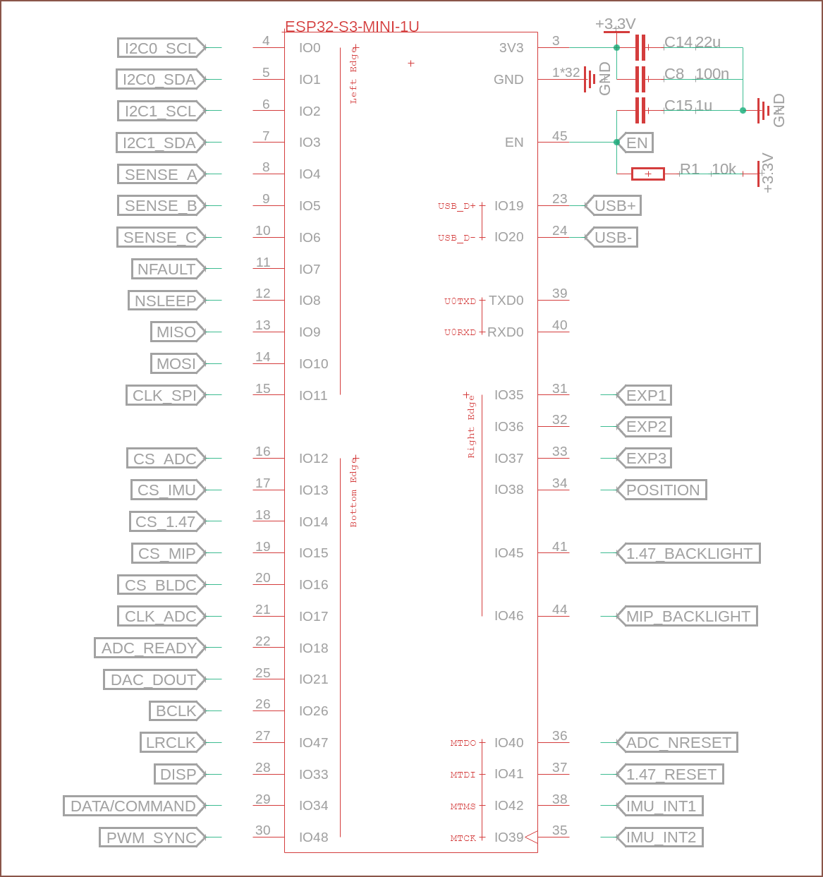
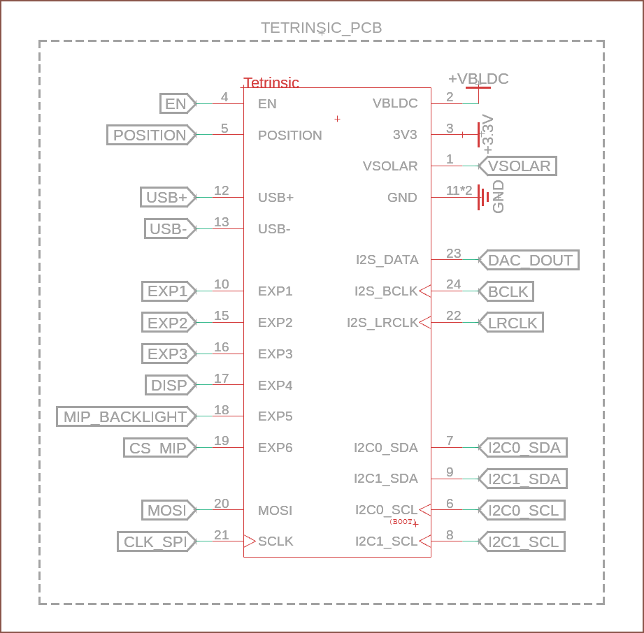
...and set up a 24P 0.7mm FPC that will be equal to the width of the PCB (which should be 17.5mm):
I2C0_SCL is connected to IO0, which is a strapping pin. If the pin is low after a reset, it'll go into boot mode. That's why there's a "(BOOT)" text under the pin.
Next Steps
Most of my research today has been around flashing multiple ESP32s. I know that there's an OTA thing, but does that mean I need to enable WiFi on all Tetrinsics momentarily? Another method could be exposing the TX/RX pins and having something like that GPIO matrix on I2C1 so that the Tetrinsic that is connected via USB can then program all the other ones
There's also the slight concern that IO3 is also a strapping pin and so it might not be a good idea to have it on I2C1.
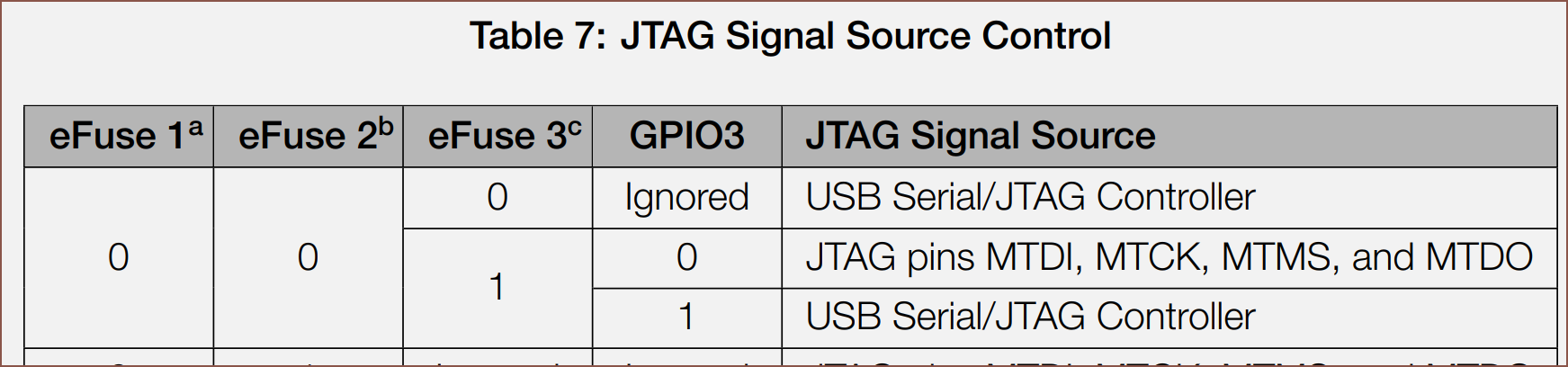
As long as I don't burn any eFuses (which are things that can't be reset to a 0 if a 1 is written to it), I should be able to use it just fine. Actually, since it'll be connected to a pull-up (and GPIO3 is ignored if either eFuse 1 or 2 is a 1), I'd still get the USB Serial mode. Thus I don't have to worry about it, unless I need to use JTAG. I don't have enough pins for it to even be an option really.
But hey 🎉🎉that LOADCELL symbol/footprint is the last one I need for this PCB design. This is a milestone I didn't even acheive on the first schematic/PCB design.
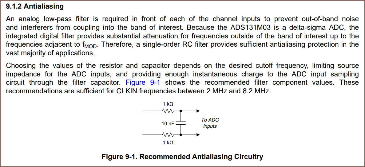
Looking back at that HX711 reference design, I remember that there were also resistors on the inputs of the reference ADS131M03 PCB. I've looked though the datasheet and it's actually mentioned right here:
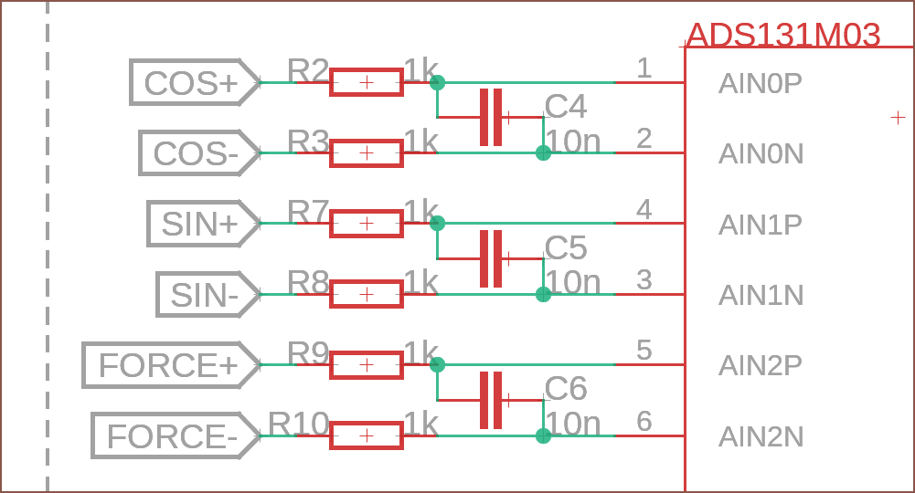
That's a lot of passives, but ok... these are 0603s too...
Discussions
Become a Hackaday.io Member
Create an account to leave a comment. Already have an account? Log In.