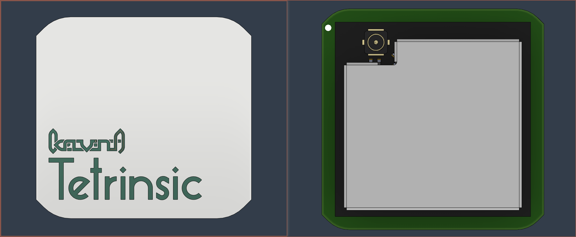
 kelvinA
It's been another 90 minutes and I've got some updates.
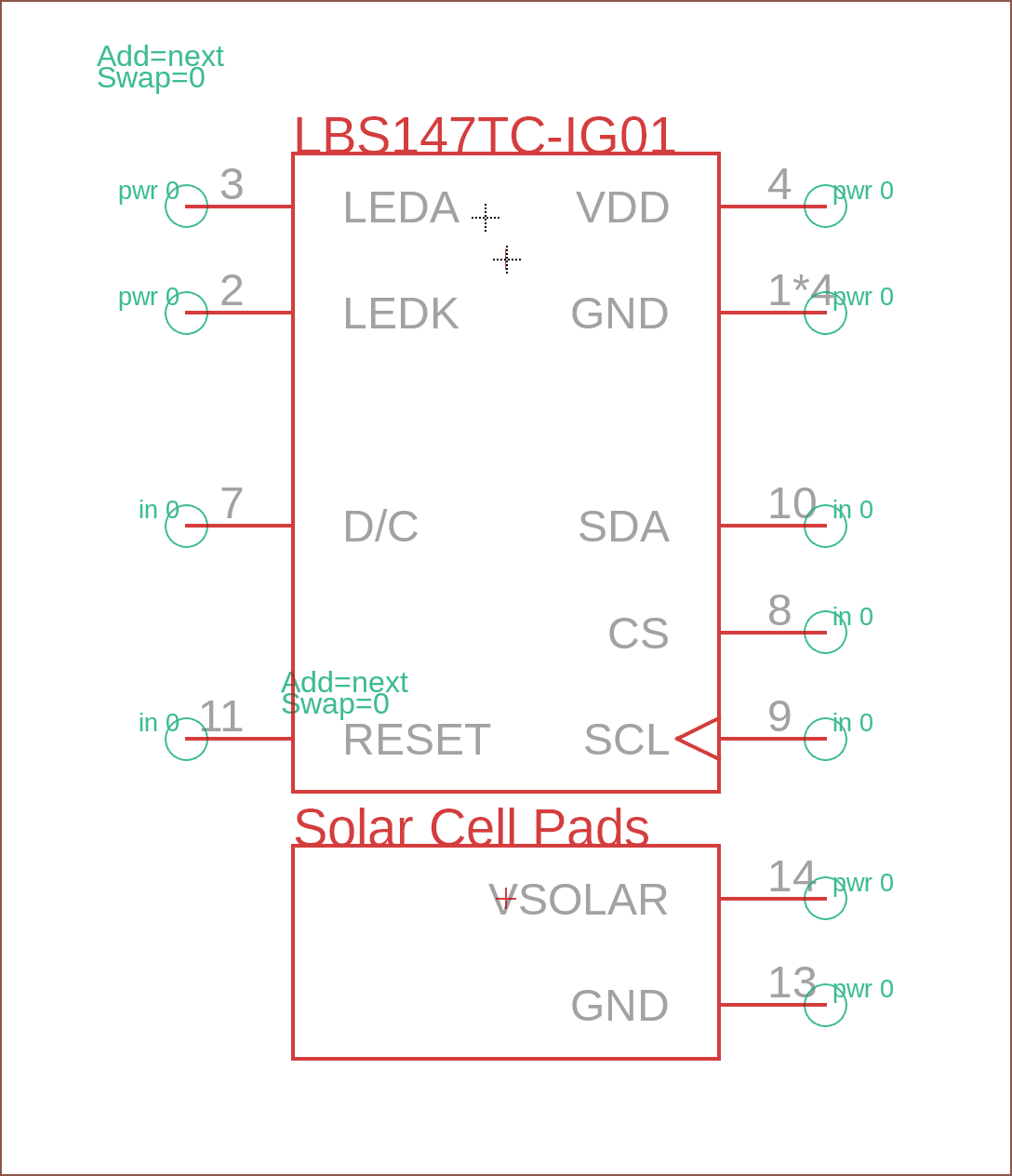
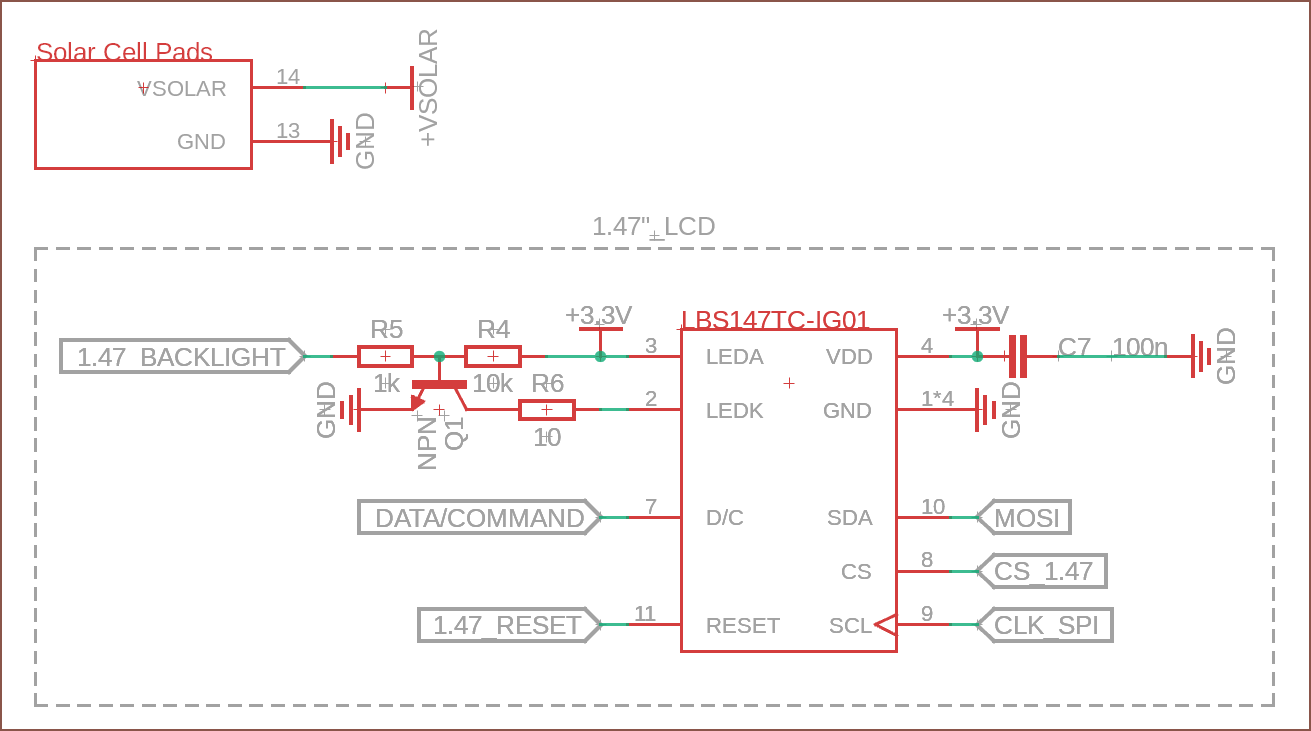
Just like with 3D CAD, I can have more than one symbol in a component. I still have the freedom to put each symbol in an arbitrary location:
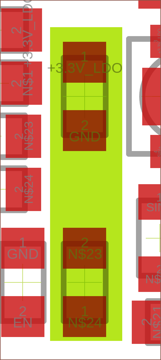
I've reordered the Tetrinsic masterpad so that VBLDC is on the right side. This also allows me to evenly split the EXP pins in half. I've put slightly lower importance pins on the right edges (POSITION / VSOLAR) in the event of manufacturing issues present at the edges of the PCB.
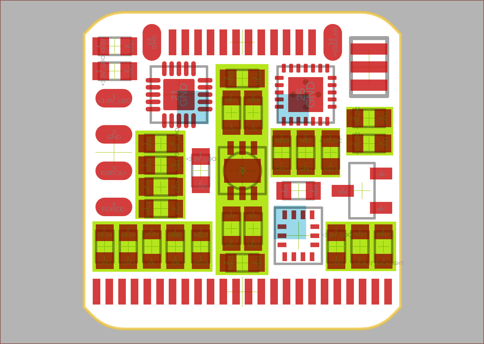
I've also been able to align components (green) and "circular pattern" the blue-marked corners of the ICs. This has the added benefit of the BLDC controller being reasonably far away from other ICs. However, it's reasonable to expect that I'll have to revert the position of the 2 passives shown below to make trace routing easier:
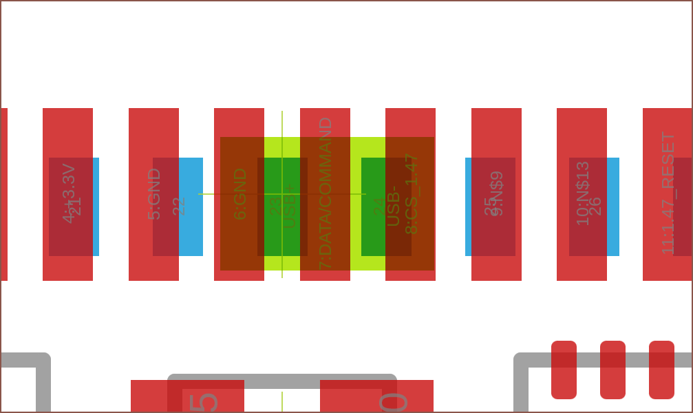
A lot of things, especially the USB data lines, are on the opposite side of where all the action is.
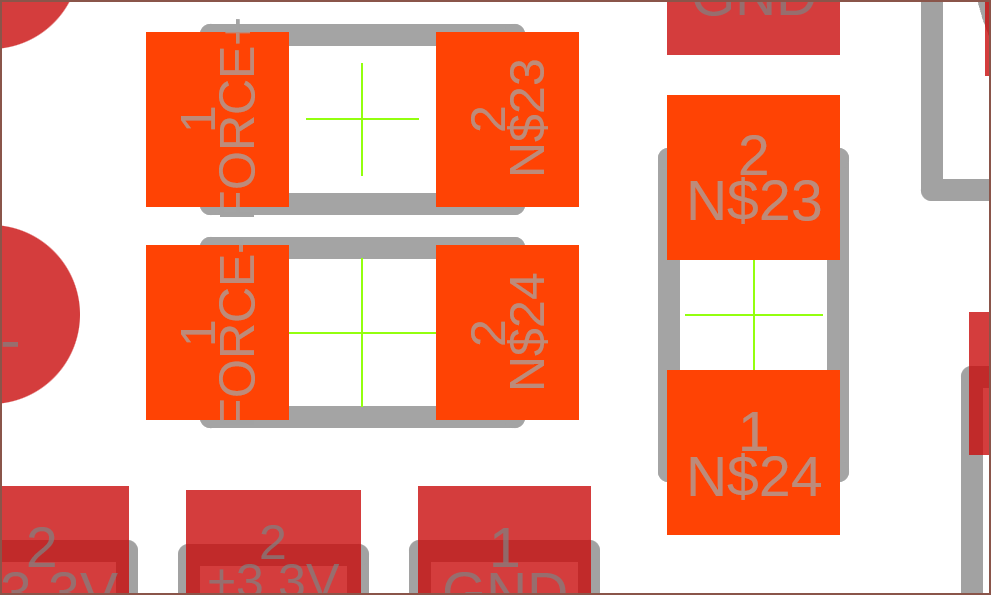
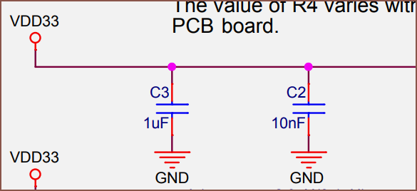
Thus, I think it makes the most sense to rotate 180...
... and then swap the order on the masterpad. The drawback is that the S3-MINI's capacitors are now on the opposite side of the board to the 3.3V input. The docs don't really mention anything about this distance, and they're still close to the 3.3V input pin in the masterpad, so I'll chance it since there's a higher chance for USB interference than things breaking due to an imperfectly clean power to the chip. It shouldn't even be that bad, since the module itself has some:
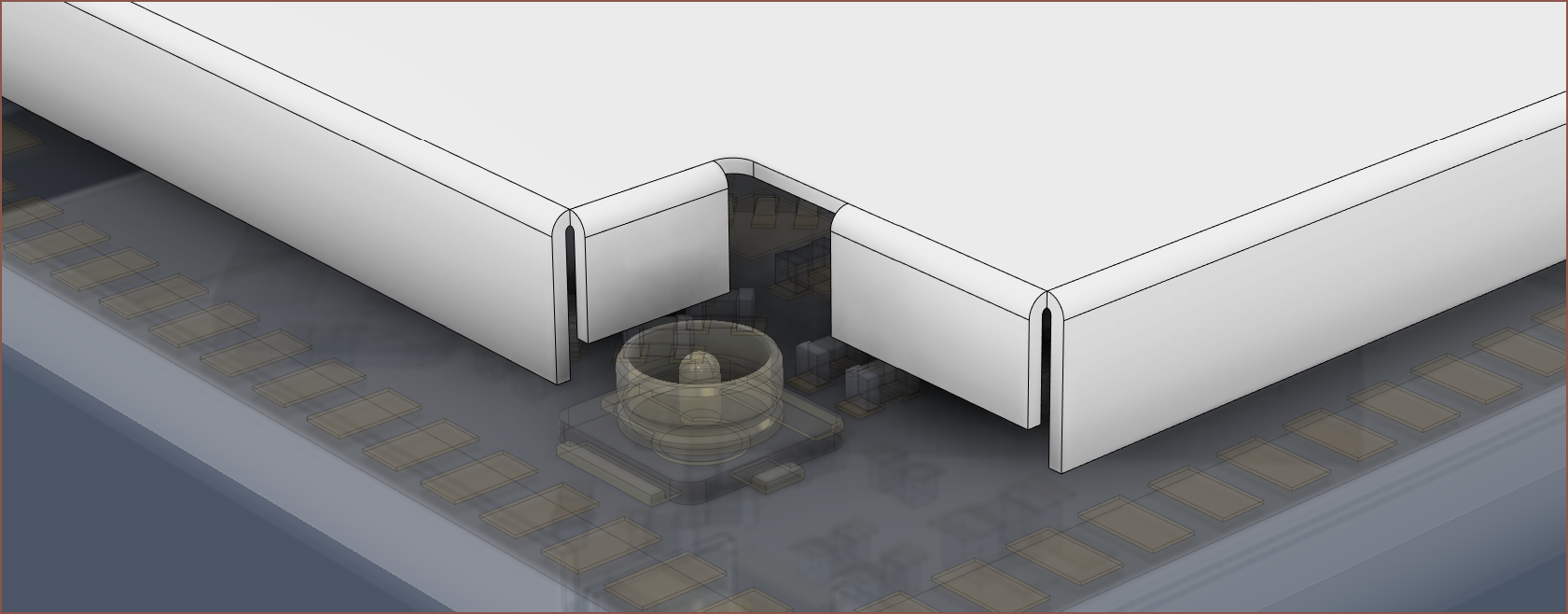
Oh, and not having these 2 walls of the MINI-1U has made me suprisingly annoyed, so I've finally spent a few minutes to model something. There's almost no images online of this angle so I'm just guessing.
Also, Fusion is going to keep requiring me to check / uncheck if I want an auto 3D model generated.
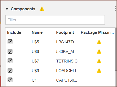
Did some reading and it seems they never got anywhere with that, so I'm just making empty 3D models:
This PCB design is really giving me a throwback vibe when I thought I could get away with a 15 x 17mm PCB:
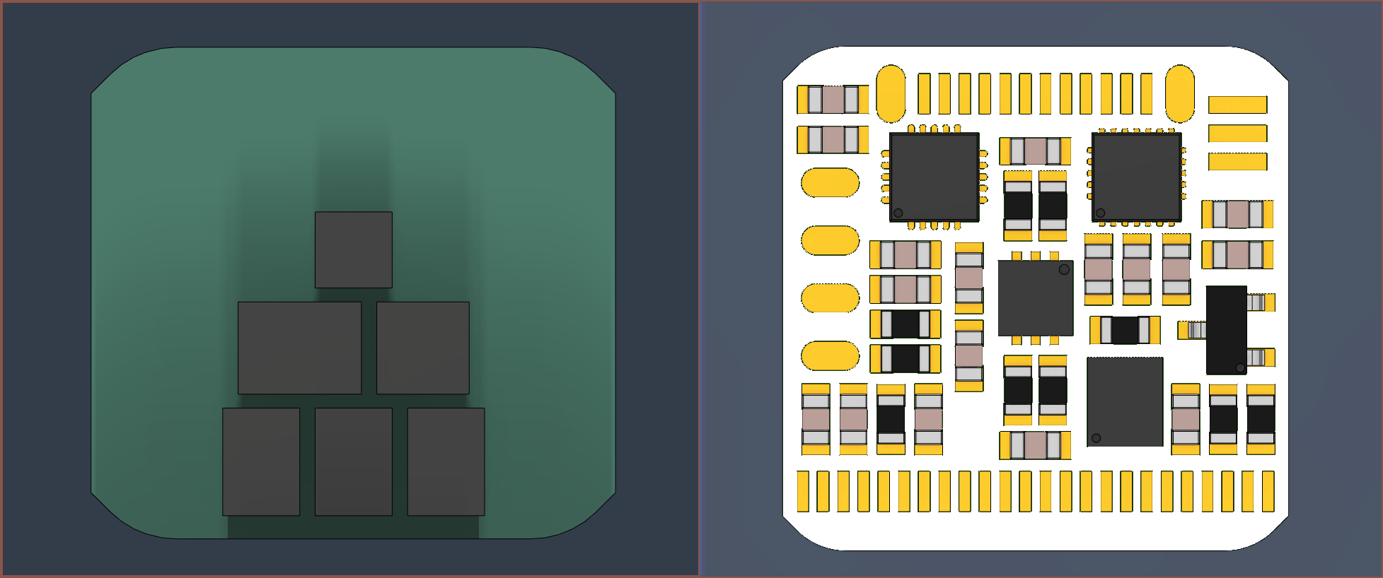
It looks just as simple from the other side though:
I still feel like vias are going to mean that I have to make the board longer than what it currently is.
Time from starting this log to finishing: 2 hours. (So everything in this log is 3.5hrs of work in total)
Discussions
Become a Hackaday.io Member
Create an account to leave a comment. Already have an account? Log In.