 kelvinA
I've seemingly spent 3+ combined hours just tweaking traces and making them look nicer:
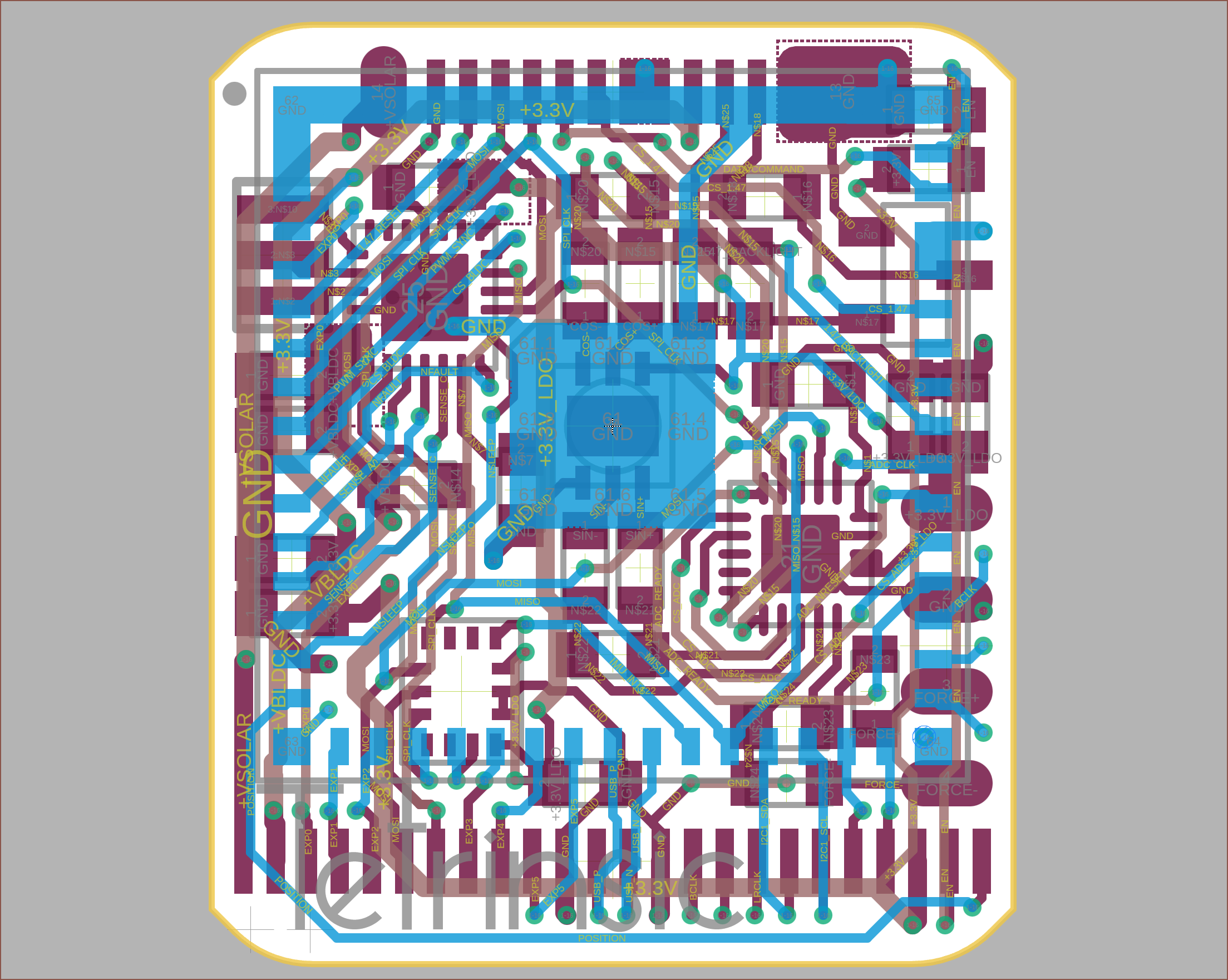 I thickened traces like the +3.3V line, as well as tweak traces like POSITIOIN so that it looked tangential to the "e" in "Tetrinsic":
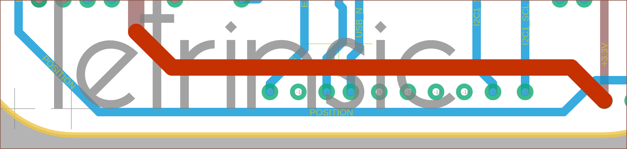
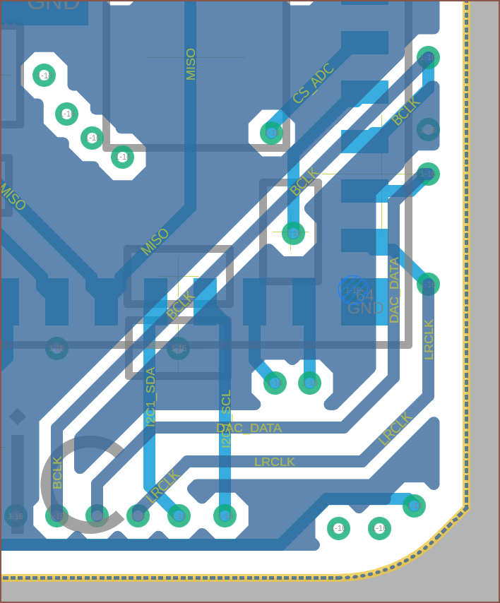
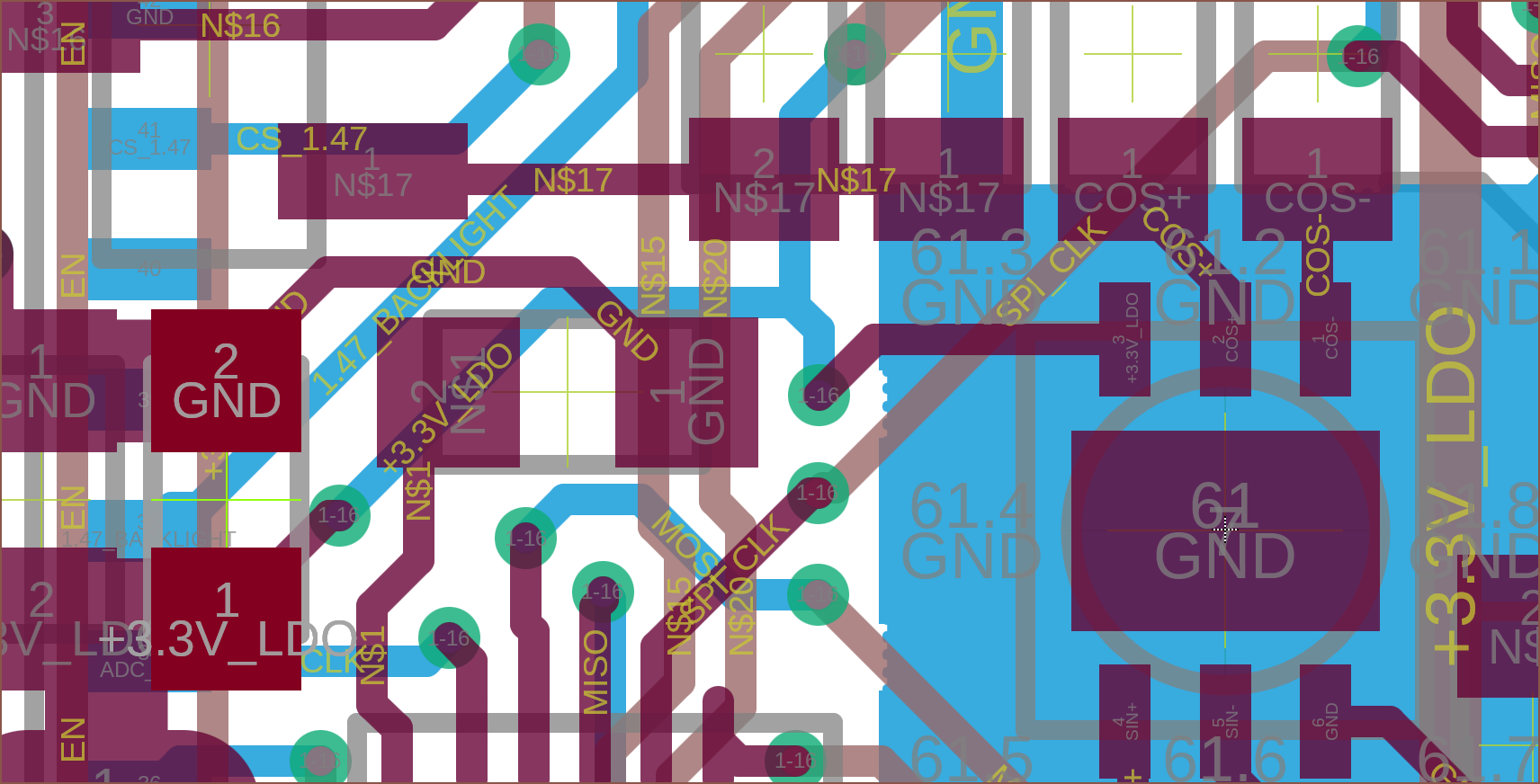
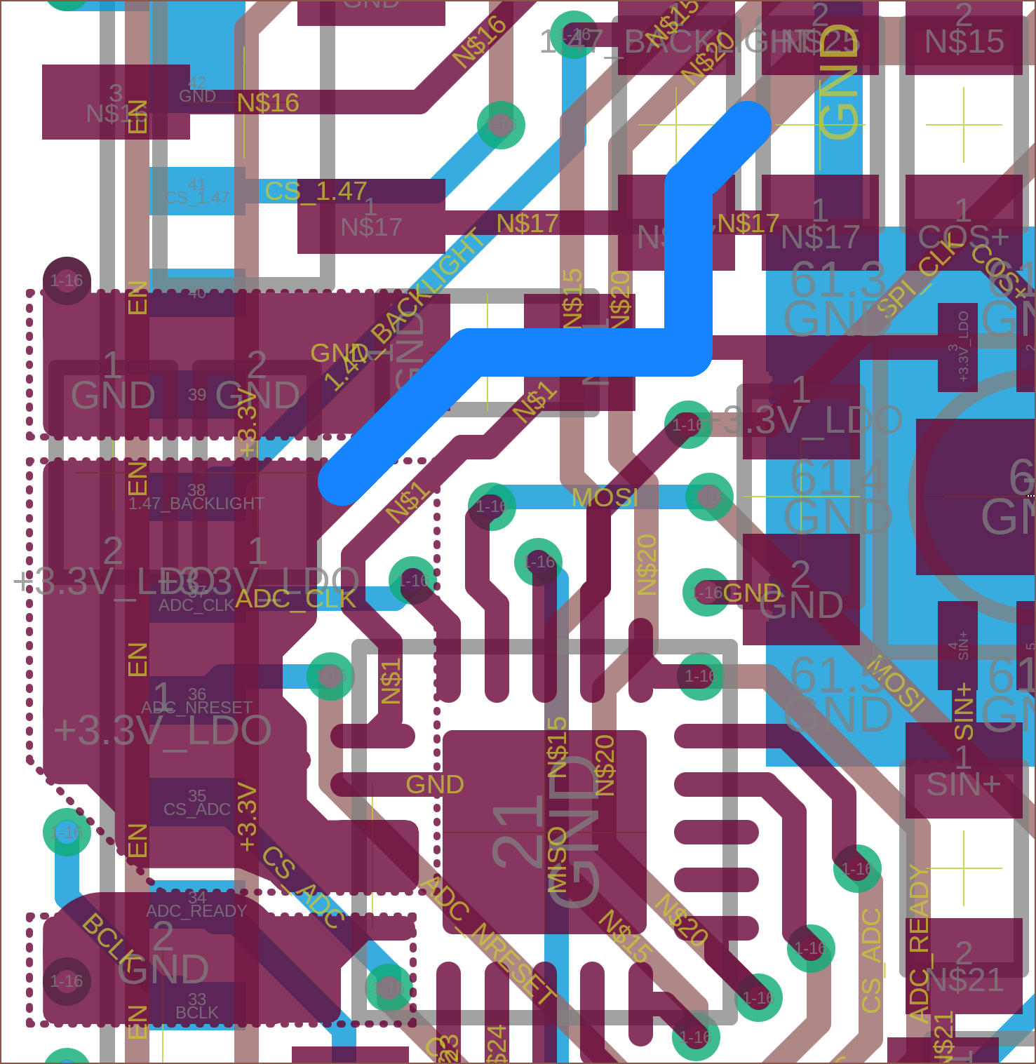
The most notable thing I've done probably is finding a way to route all the I2S pins without a via in the pad:
 I believe having a via in a large ground pad that is exposed is much better than in a small signal pad that is hidden:
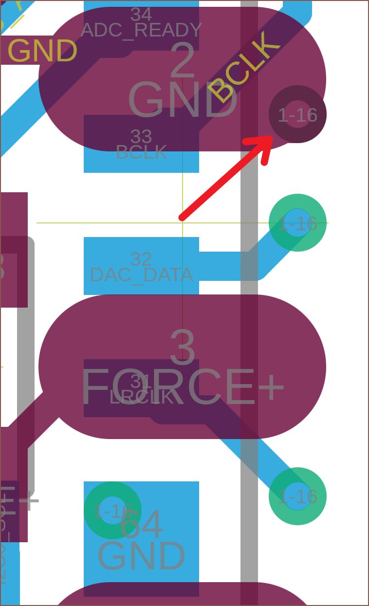
Now I'm researching the USB implementation of the S3. Basically, I just want to make sure that I can flash the board without the TX/RX pins (which looks to be the case) and that I don't get strange behaviour on the ADC, of which many pins used are also used for some "external PHY" feature:
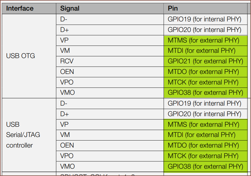
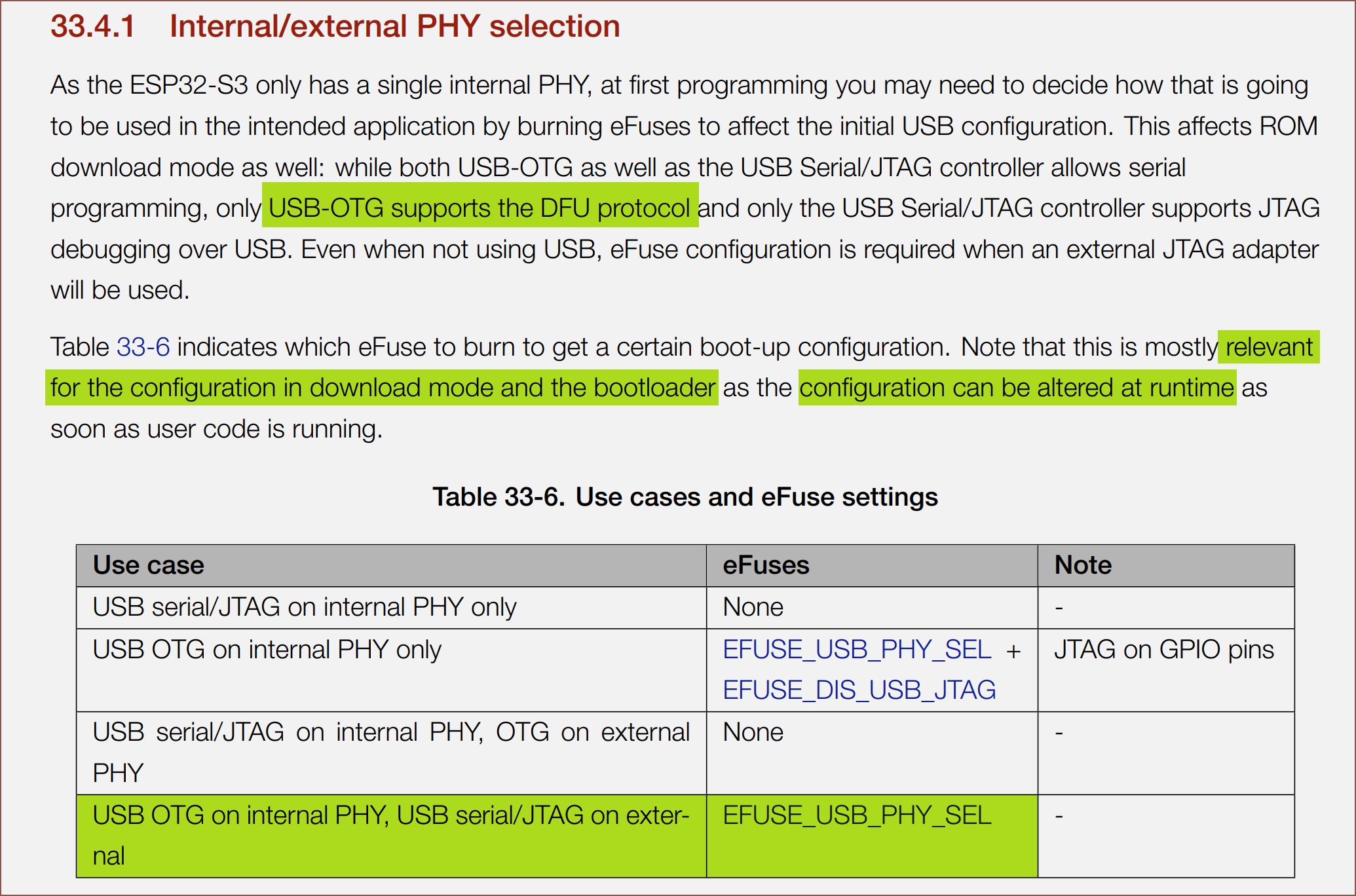
What it sounds like is that I might have to burn an efuse, but also that I might not have to since it's software configurable which USB interface is connected:
I actually thought USB was one single feature, but it's actually 2 different ones. It seems that the OTG mode allows the chip to act as both a USB host or a device, which I didn't know microcontrollers could do (note that it wasn't until late last year that I found out there were microcontrollers with native USB in the first place).
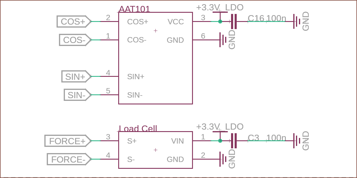
Oh and I've just realised this bypass capacitor is in the wrong location to actually do any filtering for the AAT101:
 Why do I need that again?
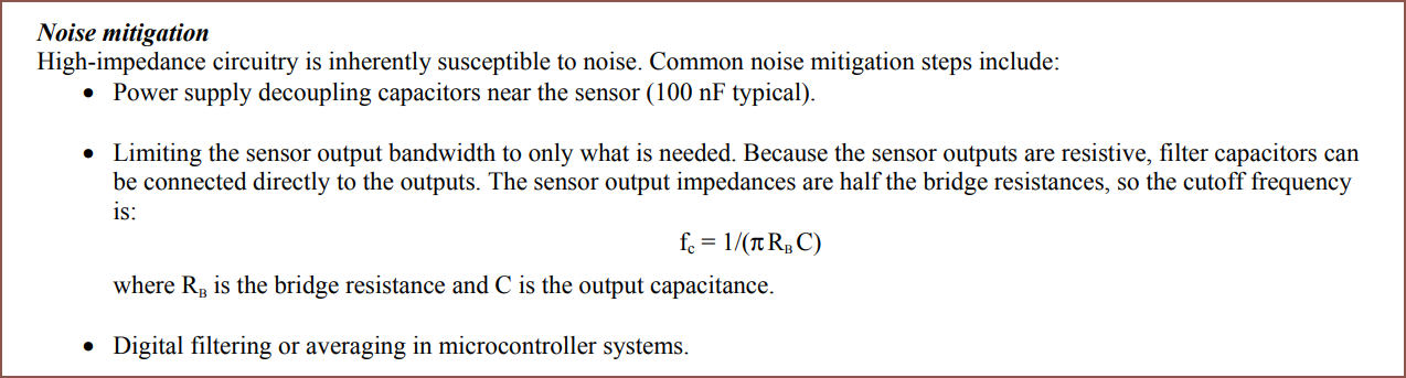
Right ok so bullet point 1 is what that bypass was supposed to do, bullet 2 are those 6 passives on the way to the ADC and the ADC itself does bullet 3. Ok... I better get a reaaaaly clean signal after I spend all the time to cram this final capacitor in...
... and I'm done.
Adding the capacitor in took like 6 minutes thanks to the power of autopush. I then spent another 20 minutes adding in fancy copper pours and thickening the +3.3V blue trace. The spacing for the AAT101 cap looks fine, but now I've noticed how I've got to be careful not to create shorts when soldering one capacitor adjacent to the BLDCC:
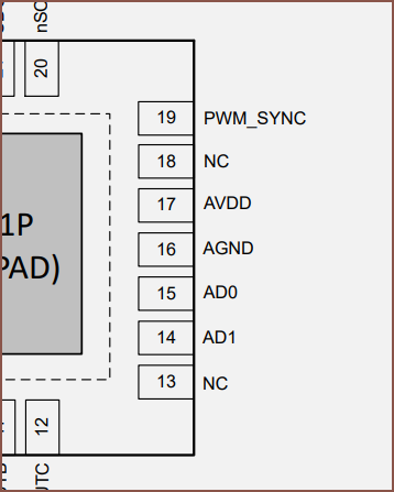 Right I forgot all about those ADn pins. Do I need those? Can they be floating or conviniently connected to the AGND next door?
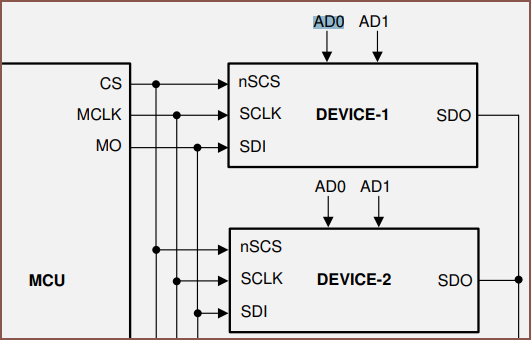 Oh cool it's like I2C on SPI, presumably to allow communications with up to 4 controllers per CS pin. Wow, Ti really made a chip with low pin utilisation in mind.
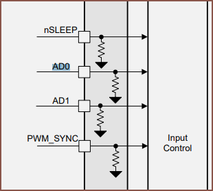 It looks like they're internally pulled down, so I probably only have to worry about accidentally shorting PWM_SYNC.
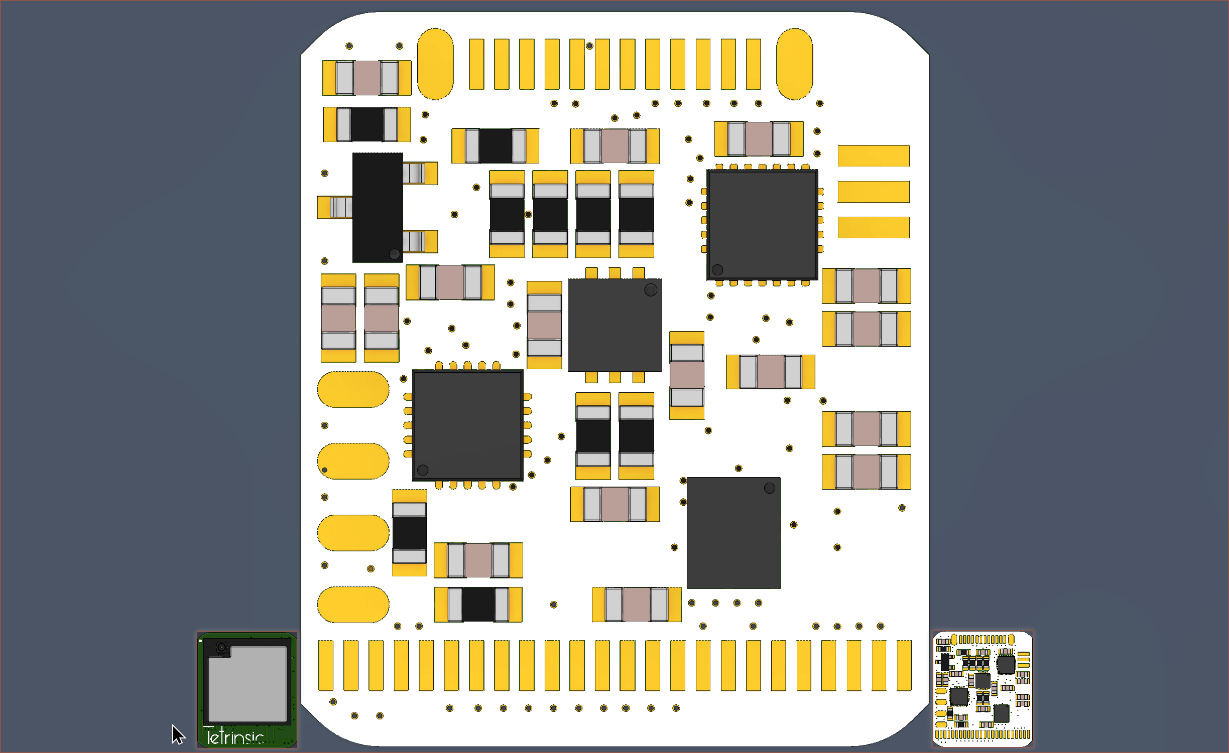
Anyway, this is the size I usually see the board on my 15.6" screen, compared to it's calibrated 1 : 1 scale size:
I think it was a good idea to switch to the single masterpad instead of trying to have 2 more interconnect FPCs. Now I can treat the implementation of Tetrinsic more like a camera module or LCD, whereby the other side of the FPC goes into a standard connector (or soldered). However, looking on AliExpress, it seems that a 0.7mm pitch connector is going to be hard to come by.
Discussions
Become a Hackaday.io Member
Create an account to leave a comment. Already have an account? Log In.