 kelvinA
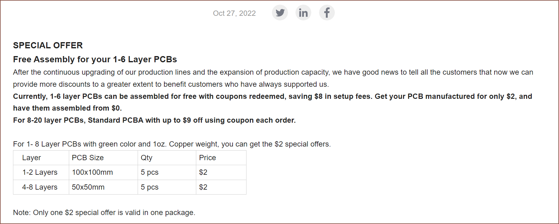
So I was on JLCPCB, looking uploading the GERBER files to see the PCB price, and I saw something:
So if I can get 5 boards pre-assembled without the processing fee, I was wondering if I should go down that option. I looked for the ICs on the top of the board, and while they existed, they were much more expensive than on Digikey/Aliexpress.
Then I got the idea that, since there's only 5 ICs total and that's where the bulk of the PCB cost is anyway, I could get the SMT service to only place the long list of passives. I soon realised that a stencil wouldn't work after components are already on it, but I remembered a project on Hackaday giving tips and tricks to high density PCB assembly and this log had a strategy that could work without the need for a stencil.
So I went into the Fusion 360 CAM Processor and I exported the BOM and Pick And Place files to CSV. Then I deleted the components I didn't need and formatted the tables like the example files provided. Fusion exports positional data just as numbers, but I found out that I can set up custom formatting in Excel. This is what I used in the 'Type:' box:
0.00"mm"
That is a number with 2 decimal places and "mm" after it, just like in the example file.
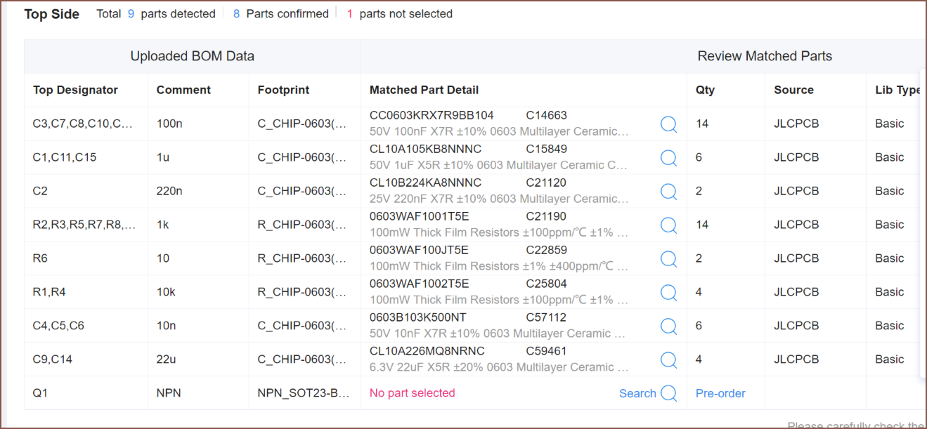
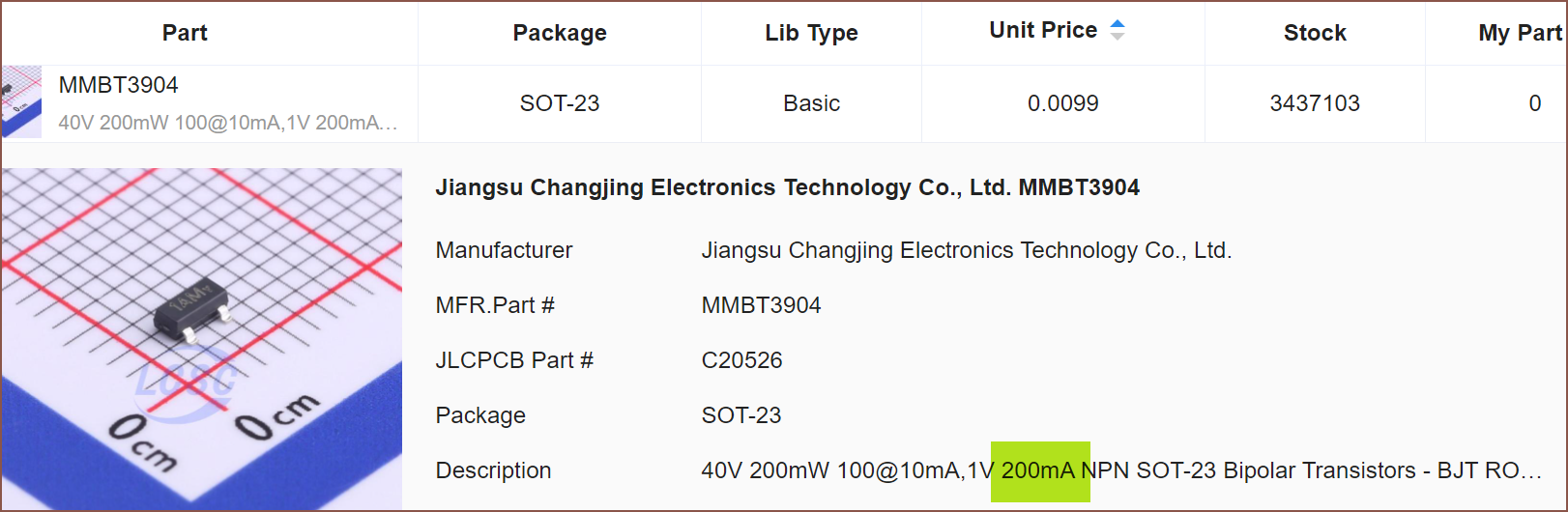
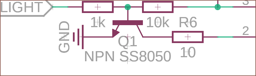
So the components actually imported and I just picked one of the first 5 options for the NPN in the "basic parts" list that had a low price and a high dissipation and sink current (all relatively speaking against the other 4 options):
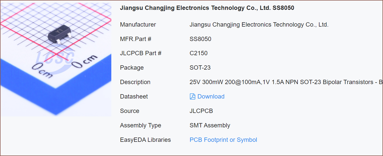
I think the backlight of the 1.47" screen takes 180mA, so I thought the cheapest part on the list was going to cut it close:
Hopefully, I can name it in the schematic and it will be automatically found in the future:
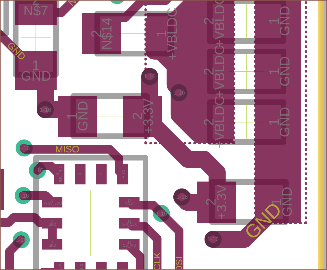
The real issue was the bulk capacitor. The 22uF capacitor for the +3.3V supply was fine, but 6.3V wouldn't be high enough for a 12V +VBLDC rail. I looked in my PCB and Me In The Past luckily designed it such that I had more space available for capacitors that I hadn't used.
So how much capacitance do I actually need, anyway? Well I don't know, couldn't really find anything on the internet, and the datasheet seems to be avoiding the question:
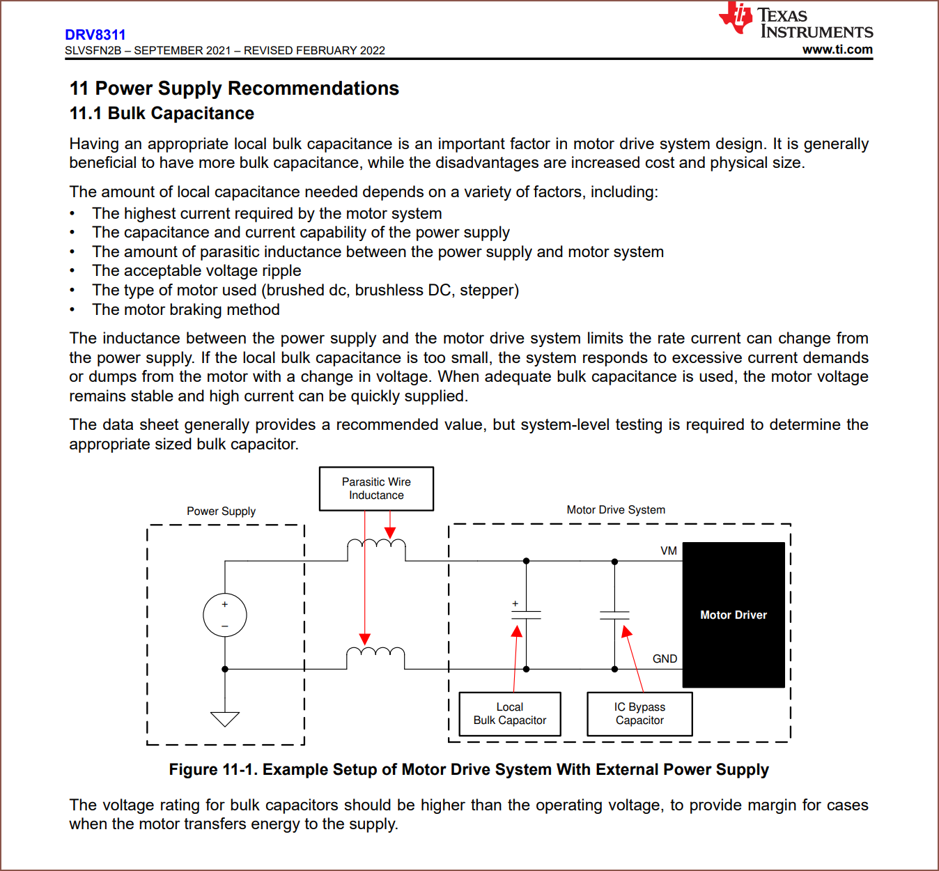
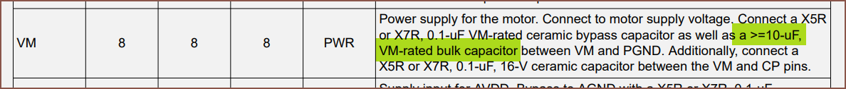
Oh wait. I didn't see that last line before the image when I was researching all this It says the capacitance right here:
Doesn't matter because, after looking through my options and finding out a 1206 was much too large...
... I found a suitable 0603:

So, assuming that the more bulk capacitance the better, I go in and start stacking capacitors in the schematic like magic circles seen in powerful incantations and then I pushpull my way to a solution:
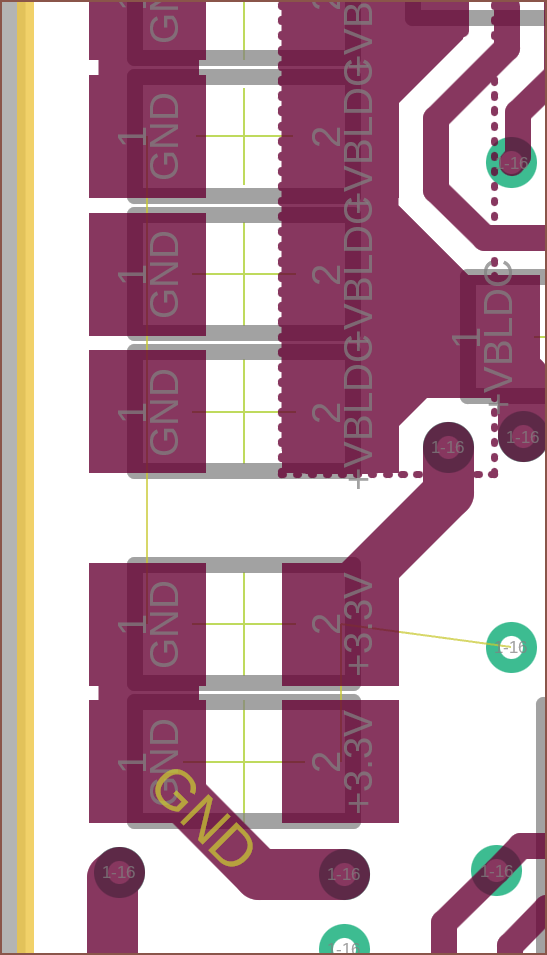
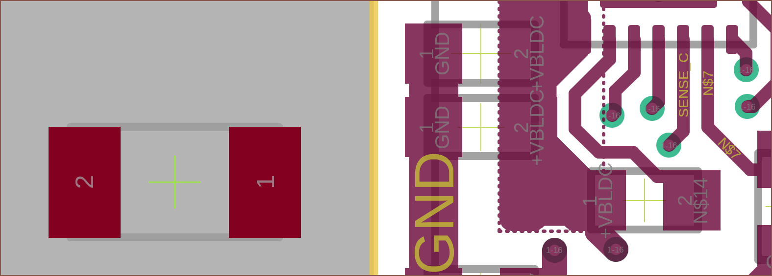
and I'm thinking "could I even get a 4th bulk capacitor in here? Wait, isn't that bottom via used for grounding the corner GND pad?"
Yes, I had 2 ground vias right next to each other.
These bulk capacitors were slightly closer to each other than any other array of passives on the board, and I really wasn't liking the idea of 3.3V merely 0.25mm away from higher voltages. It took another 10 minutes, but I was able to space everything out, remembering to make sure that the the electrons go through +3.3V pads:
Now I'm cleaning up traces before uploading to JLCPCB again.
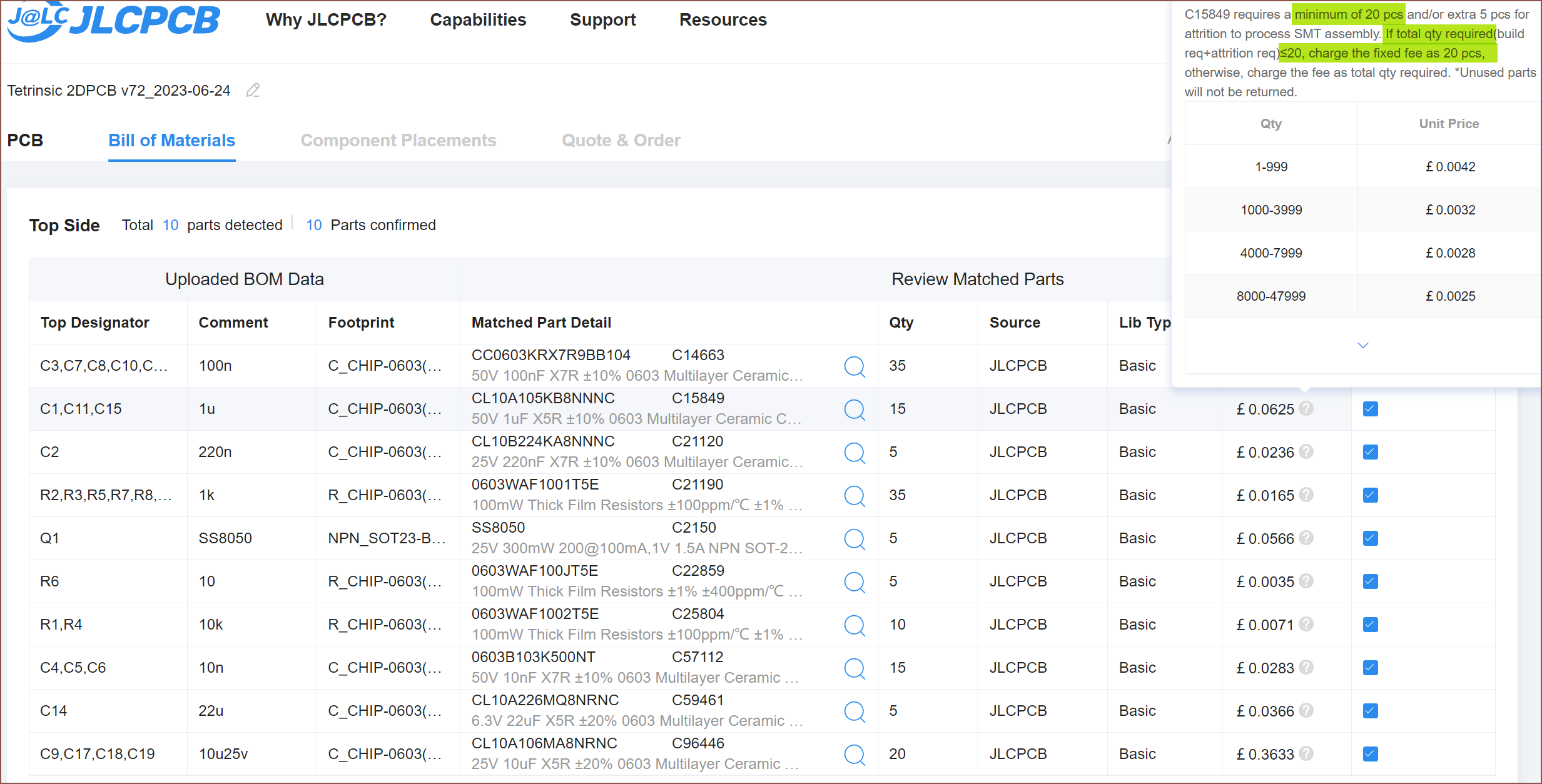
So, with some slight tweaks to the names of components, the automatic BOM generator worked. It also seems that all of them are charged at a minimum rate of 20pcs, and since only 2 components exceds that, it's certainly better to have them assemble 5pcs than 2pcs.
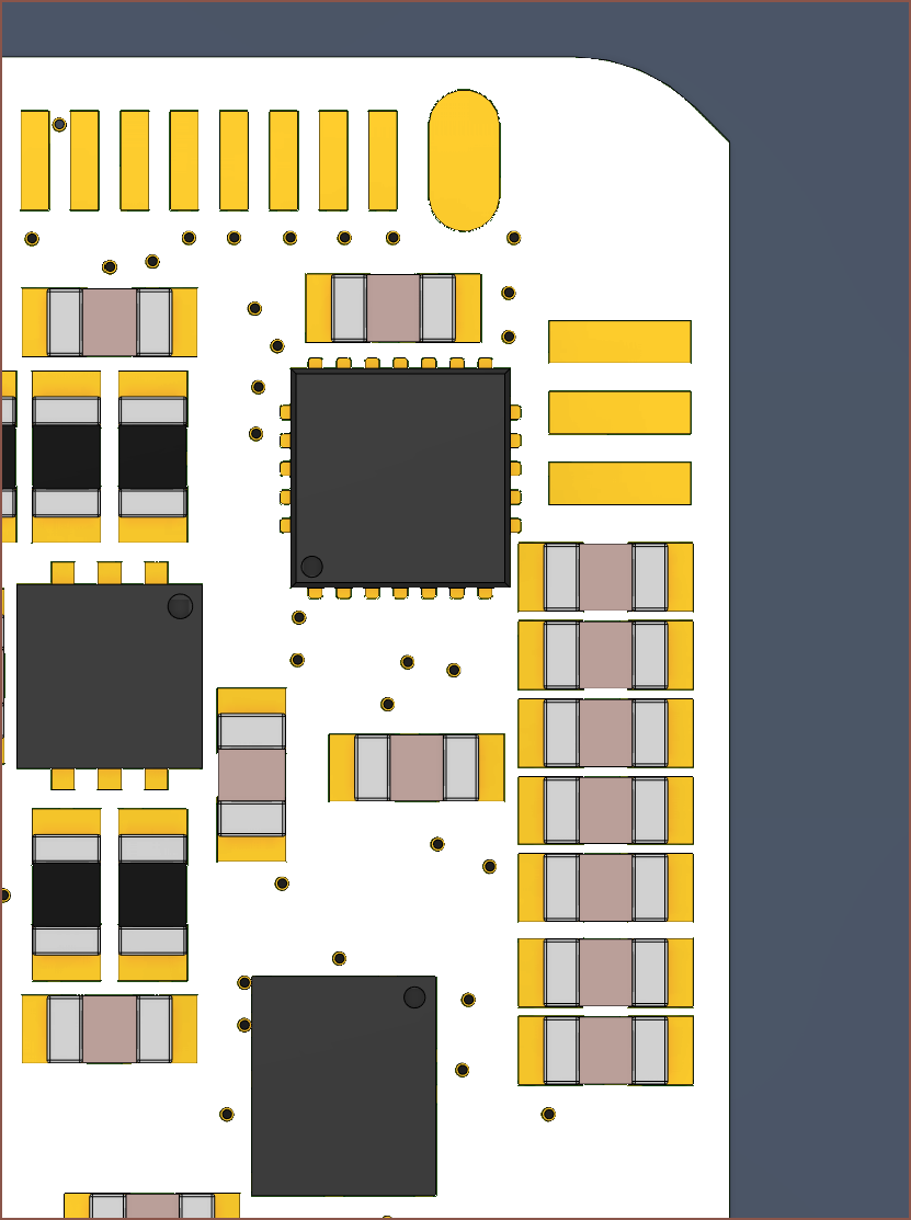
This is what my preview looks like:
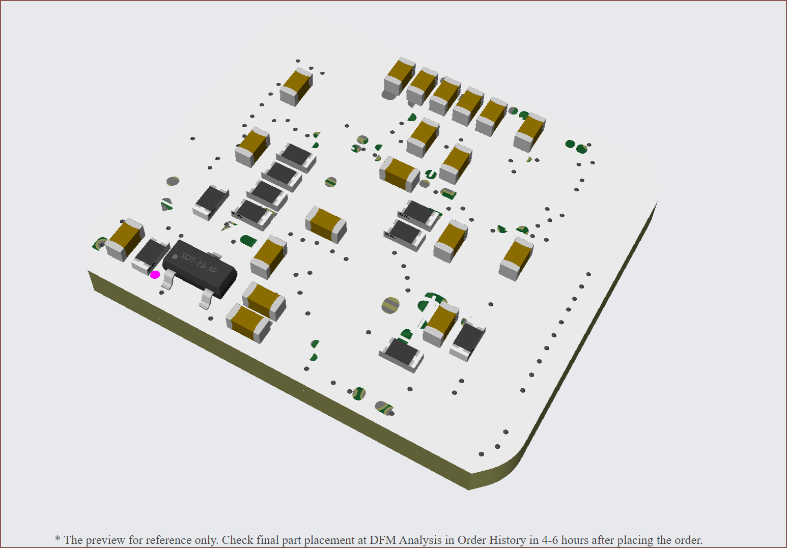
I think Fusion 360 was lazy with the silkscreen generation and it's just covered the pads. Still though, thats a lot of components that I may no long have to source and tediously place by hand if I can get the no-stencil method to work.
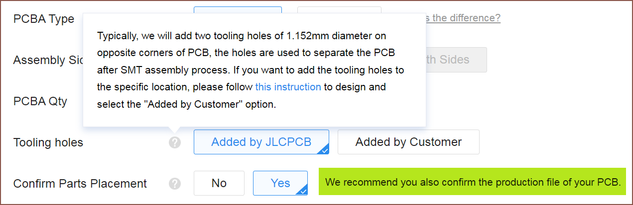
I'm wondering if I should let JLC figure something out on this tiny board or if I should add some tabs on the top / bottom that include these holes. Additionally, while it costs an extra 35p for each of these 2 confirmations, I think it's a good idea since these are 1st gen prototype boards.
Something also intersting is that I can have the SMT service or a stencil, but not both. I hope I can do that non-stencil method on the large ESP32-S3-MINI on the back.
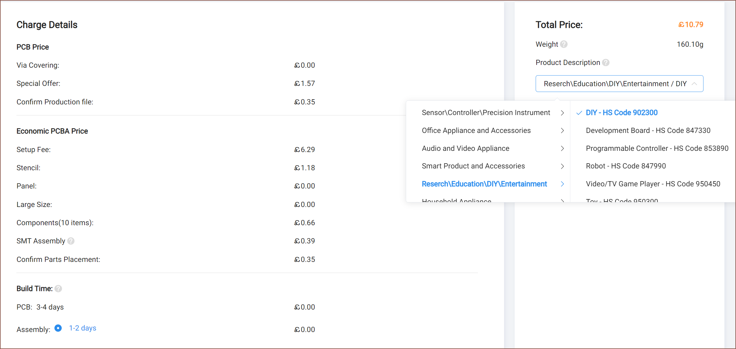
So, even with the 70p confirmation fees and the £6.29 setup fee that I should be able to redeem a coupon for, 5 assembled PCBs cost less than £11. That means I could theoretically spend as low as £3.80. The components and SMT assembly only cost a mere £1.05! That's 21p a board!
Wait... I forgot to enable settings for the board itself.
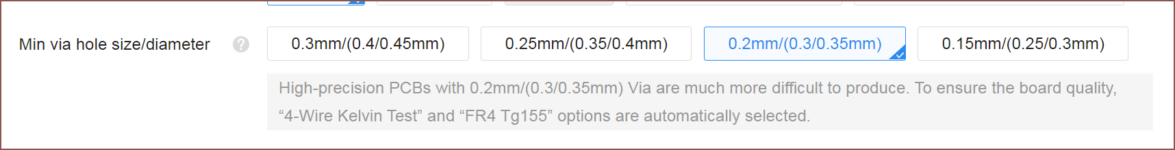
That sounds expensive. it kinda seems that I could still have my 0.4 outer diameter vias though. It also seems that there's a price bump when I opt for a 0.8mm thick PCB as opposed to 1mm and up. I'm not that critical of 0.2mm. Anyway, I've got to go in and change the minimum via holes to 0.3mm. Most of them are converting, but there are some that dont'.
Discussions
Become a Hackaday.io Member
Create an account to leave a comment. Already have an account? Log In.